- 您現(xiàn)在的位置:買賣IC網(wǎng) > PDF目錄383239 > L6928D013TR (意法半導(dǎo)體) HIGH EFFICIENCY MONOLITHIC SYNCHRONOUS STEP DOWN REGULATOR PDF資料下載
參數(shù)資料
L6928D
2/9
Table 2. Absolute Maximum Ratings
Symbol
V
6
Input voltage
V
5
Output switching voltage
V
1
Shutdown
V
3
Feedback voltage
V
2
Error amplifier output voltage
V
8
PGOOD
V
7
Synchronization mode selector
Ptot
Power dissipation at Tamb=70
°
C
Tj
Junction operating temperature range
Tstg
Storage temperature range
LX Pin
Maximum Withstanding Voltage Range Test Condition: CDF-
AEC-Q100-002- “Human Body Model” Acceptance Criteria:
“Normal Performance’
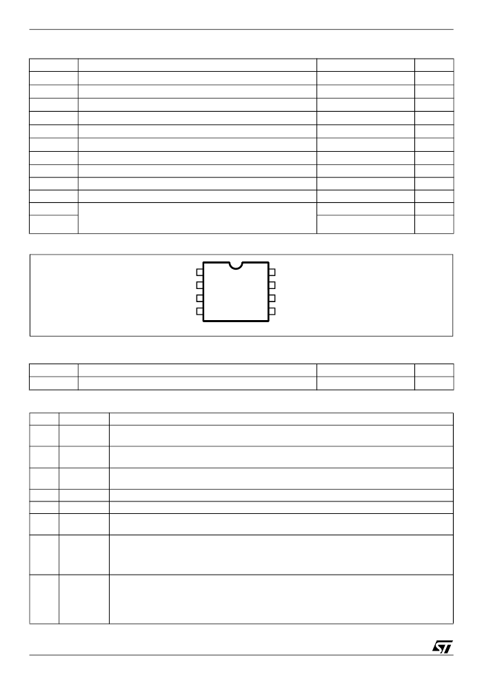
Figure 3. Pin Connection
Table 3. Thermal Data
Symbol
R
th j-amb
Table 4. Pin Functions
N
Name
1
RUN
Parameter
Value
-0.3 to 6
Unit
V
-1 to V
CC
-0.3 to V
CC
-0.3 to V
CC
-0.3 to V
CC
-0.3 to V
CC
-0.3 to V
CC
0.45
-40 to 150
-65 to 150
±1000
±2000
V
V
V
V
V
V
W
°
C
°
C
V
V
Other pins
Parameter
Value
180
Unit
°
C/W
Thermal Resistance Junction to Ambient
Description
Shutdown input. When connected to a low level (lower than 0.4V) the device stops working.
When high (higher than 1.3V) the device is enabled.
Error amplifier output. A compensation network has to be connected to this pin. Usually a
220pF capacitor is enough to guarantee the loop stability.
Error amplifier inverting input. The output voltage can be adjusted from 0.6V up to the input
voltage by connecting this pin to an external resistor divider.
Ground.
Switch output node. This pin is internally connected to the drain of the internal switches.
Input voltage. The start up input voltage is 2.2V (typ) while the operating input voltage range is
from 2V to 5.5V. An internal UVLO circuit realizes a 100mV (typ.) hysteresis.
Operating mode selector input. When high (higher than 1.3V) the Low Consumption Mode is
selected. When low (lower than 0.5V) the Low Noise Mode is selected. If connected with an
appropriate external synchronization signal (from 1MHz up to 2MHz) the internal
synchronization circuit is activated and the device works at the same switching frequency.
Power good comparator output. It is an open drain output. A pull-up resistor should be
connected between PGOOD and VOUT (or VCC depending on the requirements). The pin is
forced low when the output voltage is lower than 90% of the regulated output voltage and goes
high when the output voltage is greater than 90% of the regulated output voltage. If not used the
pin can be left floating.
2
COMP
3
VFB
4
5
6
GND
LX
VCC
7
SYNC
8
PGOOD
RUN
COMP
VFB
GND
1
3
2
4
LX
V
CC
SYNC
PGOOD
8
7
6
5
D01IN1239AMOD
相關(guān)PDF資料 |
PDF描述 |
|---|---|
| L6932D12TR | HIGH PERFORMANCE 2A ULDO LINEAR REGULATOR |
| L6932D25TR | HIGH PERFORMANCE 2A ULDO LINEAR REGULATOR |
| L6932 | HIGH PERFORMANCE 2A ULDO LINEAR REGULATOR |
| L6932D12 | HIGH PERFORMANCE 2A ULDO LINEAR REGULATOR |
| L6932D18 | HIGH PERFORMANCE 2A ULDO LINEAR REGULATOR |
相關(guān)代理商/技術(shù)參數(shù) |
參數(shù)描述 |
|---|---|
| L6928Q1 | 功能描述:直流/直流開關(guān)調(diào)節(jié)器 Hi EFFICIENCY MONOLITHIC SYNC RoHS:否 制造商:International Rectifier 最大輸入電壓:21 V 開關(guān)頻率:1.5 MHz 輸出電壓:0.5 V to 0.86 V 輸出電流:4 A 輸出端數(shù)量: 最大工作溫度: 安裝風(fēng)格:SMD/SMT 封裝 / 箱體:PQFN 4 x 5 |
| L6928Q1TR | 功能描述:直流/直流開關(guān)調(diào)節(jié)器 HIGH EFFICIENCY MONO LITHIC SYNCHRONOUS RoHS:否 制造商:International Rectifier 最大輸入電壓:21 V 開關(guān)頻率:1.5 MHz 輸出電壓:0.5 V to 0.86 V 輸出電流:4 A 輸出端數(shù)量: 最大工作溫度: 安裝風(fēng)格:SMD/SMT 封裝 / 箱體:PQFN 4 x 5 |
| L6928TQ1TR | 制造商:STMICROELECTRONICS 制造商全稱:STMicroelectronics 功能描述:High efficiency monolithic synchronous step down regulator |
| L6928TR | 制造商:STMICROELECTRONICS 制造商全稱:STMicroelectronics 功能描述:High efficiency monolithic synchronous step down regulator |
| L-693 | 制造商:RHOMBUS-IND 制造商全稱:Rhombus Industries Inc. 功能描述:Common Mode Choke |
發(fā)布緊急采購(gòu),3分鐘左右您將得到回復(fù)。