- 您現在的位置:買賣IC網 > PDF目錄383235 > L6204D (意法半導體) DMOS DUAL FULL BRIDGE DRIVER PDF資料下載
參數資料
| 型號: | L6204D |
| 廠商: | 意法半導體 |
| 英文描述: | DMOS DUAL FULL BRIDGE DRIVER |
| 中文描述: | 偶的DMOS全橋驅動器 |
| 文件頁數: | 6/10頁 |
| 文件大?。?/td> | 197K |
| 代理商: | L6204D |
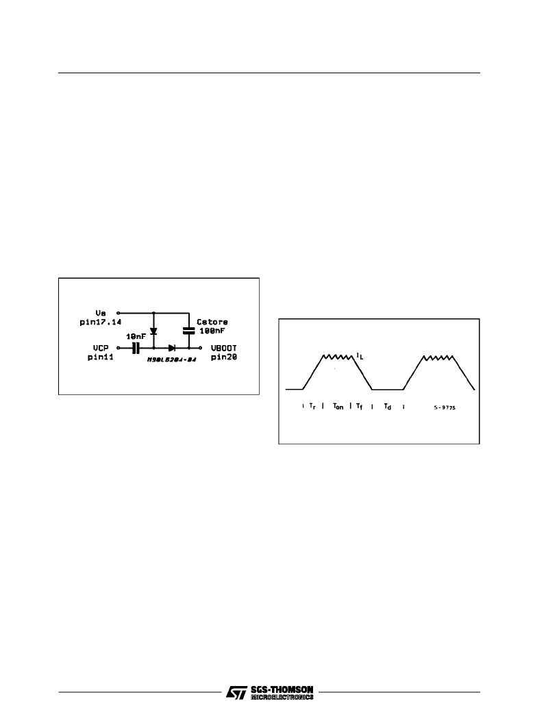
a voltage higher than V
S
is supplied on pin 20
(V
boot
). This bootstrap voltage is not needed for
the lower power DMOS transistor because their
sources are grounded. To produce this voltage a
charge pump method is used and mAde by two
external capacitors and two diodes. It can supply
the 4 driving blocksof the high side drivers. Using
an external capacitor the turn-on speed of the
high side driver is very high; furthermore with dif-
ferent capacitance values it is possible to adapt
the device to different switching frequencies. It is
also possible to operate two or more L6204s us-
ing only 2 diodes and 2 capacitance for all the
ICs; all the Vboot pins are connectedto the C
store
capacitance while the pin 11 (VCP) of just one
L6204 is connect to C
pump
, obviously all the
L6204 ICs have to be connected to the same V
S
.
(see fig. 4)
DEAD TIME
To protect the device against simultaneous con-
duction in both arms of the bridge and the result-
ing rail-to-rail short, the logic circuits provide a
dead time.
THERMAL PROTECTION
A thermal protection circuit has been included
that will disable the device if the junction tempera-
ture reaches 150
°
C. When the temperature has
fallen to a safe level the device restarts under the
control of the input and enable signals.
APPLICATION INFORMATION
RECIRCULATION
During recirculation with the ENABLE input high,
the voltage drop across the transistor is R
DS(ON)
.
I
L
for voltages less than 0.7 V and is clamped at a
voltage depending on the characteristics of the
source-drain diode for greater voltages. Although
the device is protected against cross conduction,
current spikes can appear on the current sense
pin due to charge/dischargephenomena in the in-
trinsic source drain capacitances. In the applica-
tion this does not cause any problems because
the voltage created across the sense resistor is
usuallymuch less thanthe peak value, althougha
small RC filtercan be added if necessary.
POWER DISSIPATION (each bridge)
In order to achieve the high performance provided
by the L6204 some attention must be paid to en-
sure that it has an adequate PCB area to dissi-
pate the heat. The first stage of any thermal de-
sign is to calculate the dissipated power in the
application, for this example the half step opera-
tion shown in figure 5 is considered.
RISE TIMET
r
When an arm of the half bridge is turned on cur-
rent begins to flow in the inductive load until the
maximum current I
L
is reached after a time T
r
.
The dissipatedenergy E
OFF/ON
is in thiscase :
E
OFF/ON
= [R
DS(ON)
I
L2
T
r
]
2/3
ON TIME T
ON
During this time the energy dissipated is due to
the ON resistance of the transistors E
ON
and the
commutationE
COM
. As two of the POWER DMOS
transistors are ON E
ON
is given by :
E
ON
= I
L2
R
DS(ON)
2
T
ON
In the commutationthe energydissipated is :
E
COM
= V
S
IL
T
COM
f
SWITCH
T
ON
Where :
T
COM
= CommutationTime and itis assumedthat;
T
COM
= T
TURN-ON
= T
TURN-OFF
= 100 ns
f
SWITCH
= Chopperfrequency
FALL TIME T
f
For this example it is assumed that the energy
dissipated in this part of the cycle takes the same
form as thatshown for the risetime :
E
ON/OFF
= [R
DS(ON)
I
L
2
T
f
]
2/3
Figure4
Figure 5
L6204
6/10
相關PDF資料 |
PDF描述 |
|---|---|
| L6205 | DMOS DUAL FULL BRIDGE DRIVER |
| L6205D | DMOS DUAL FULL BRIDGE DRIVER |
| L6205N | DMOS DUAL FULL BRIDGE DRIVER |
| L6205PD | DMOS DUAL FULL BRIDGE DRIVER |
| L6206 | CAP CER 110PF 100V 5% C0G 0805 |
相關代理商/技術參數 |
參數描述 |
|---|---|
| L6204D013TR | 功能描述:馬達/運動/點火控制器和驅動器 Dual Full Bridge RoHS:否 制造商:STMicroelectronics 產品:Stepper Motor Controllers / Drivers 類型:2 Phase Stepper Motor Driver 工作電源電壓:8 V to 45 V 電源電流:0.5 mA 工作溫度:- 25 C to + 125 C 安裝風格:SMD/SMT 封裝 / 箱體:HTSSOP-28 封裝:Tube |
| L6205 | 制造商:STMICROELECTRONICS 制造商全稱:STMicroelectronics 功能描述:DMOS DUAL FULL BRIDGE DRIVER |
| L6205D | 功能描述:馬達/運動/點火控制器和驅動器 Dual Full Bridge RoHS:否 制造商:STMicroelectronics 產品:Stepper Motor Controllers / Drivers 類型:2 Phase Stepper Motor Driver 工作電源電壓:8 V to 45 V 電源電流:0.5 mA 工作溫度:- 25 C to + 125 C 安裝風格:SMD/SMT 封裝 / 箱體:HTSSOP-28 封裝:Tube |
| L6205D013TR | 功能描述:馬達/運動/點火控制器和驅動器 Dual Full Bridge RoHS:否 制造商:STMicroelectronics 產品:Stepper Motor Controllers / Drivers 類型:2 Phase Stepper Motor Driver 工作電源電壓:8 V to 45 V 電源電流:0.5 mA 工作溫度:- 25 C to + 125 C 安裝風格:SMD/SMT 封裝 / 箱體:HTSSOP-28 封裝:Tube |
| L6205N | 功能描述:馬達/運動/點火控制器和驅動器 Dual Full Bridge RoHS:否 制造商:STMicroelectronics 產品:Stepper Motor Controllers / Drivers 類型:2 Phase Stepper Motor Driver 工作電源電壓:8 V to 45 V 電源電流:0.5 mA 工作溫度:- 25 C to + 125 C 安裝風格:SMD/SMT 封裝 / 箱體:HTSSOP-28 封裝:Tube |
發(fā)布緊急采購,3分鐘左右您將得到回復。