- 您現(xiàn)在的位置:買賣IC網(wǎng) > PDF目錄384543 > ISPLSI3256A-70LQI (LATTICE SEMICONDUCTOR CORP) In-System Programmable High Density PLD PDF資料下載
參數(shù)資料
| 型號: | ISPLSI3256A-70LQI |
| 廠商: | LATTICE SEMICONDUCTOR CORP |
| 元件分類: | PLD |
| 英文描述: | In-System Programmable High Density PLD |
| 中文描述: | EE PLD, 18 ns, PQFP160 |
| 封裝: | PLASTIC, QFP-160 |
| 文件頁數(shù): | 11/13頁 |
| 文件大?。?/td> | 163K |
| 代理商: | ISPLSI3256A-70LQI |
Specifications
ispLSI 3256A
11
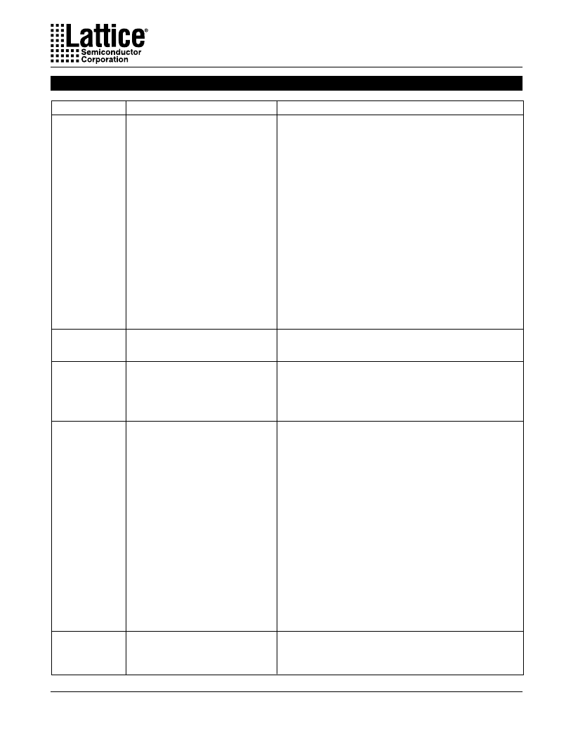
Pin Description
Dedicated Clock inputs. These clock inputs are connected to one of the
clock inputs of all the I/O cells in the device.
Dedicated Clock inputs. These clock inputs are connected to one of the
clock inputs of all the GLBs on the device.
Active Low (0) Reset pin which resets all of the GLB and I/O registers in
the device.
Input
–
Dedicated in-system programming enable input pin. When this pin is high,
the BSCAN TAP controller pins TMS, TDI, TDO and TCK are enabled. When this
pin is brought low, the ISP state machine control pins MODE, SDI, SDO and
SLCK are enabled. High-to-low transition of this pin will put the device in the
programming mode and put all I/O pins in high-Z state.
Input/Output Pins - These are the general purpose I/O pins used by the
logic array.
NAME
Table 2-0002/3256A.a
PQFP/MQFP PIN NUMBERS
DESCRIPTION
25,
32,
37,
42,
48,
54,
59,
65,
70,
76,
82,
87,
93,
106,
113,
118,
123,
129,
135,
140,
146,
152,
157,
3,
8,
15,
26,
33,
38,
43,
49,
55,
60,
66,
72,
77,
83,
88,
94,
108,
114,
119,
124,
130,
136,
141,
147,
153,
158,
4,
9,
16,
28,
34,
39,
44,
50,
56,
61,
67,
73,
78,
84,
89,
95,
109,
115,
120,
126,
132,
137,
142,
148,
154,
159,
5,
11,
17
I/O 0 - I/O 4
I/O 5 - I/O 9
I/O 10 - I/O 14
I/O 15 - I/O 19
I/O 20 - I/O 24
I/O 25 - I/O 29
I/O 30 - I/O 34
I/O 35 - I/O 39
I/O 40 - I/O 44
I/O 45 - I/O 49
I/O 50 - I/O 54
I/O 55 - I/O 59
I/O 60 - I/O 64
I/O 65 - I/O 69
I/O 70 - I/O 74
I/O 75 - I/O 79
I/O 80 - I/O 84
I/O 85 - I/O 89
I/O 90 - I/O 94
I/O 95 - I/O 99
I/O 100 - I/O 104
I/O 105 - I/O 109
I/O 110 - I/O 114
I/O 115 - I/O 119
I/O 120 - I/O 124
I/O 125 - I/O 127
29,
35,
40,
46,
52,
57,
62,
68,
74,
79,
85,
90,
96,
110,
116,
121,
127,
133,
138,
144,
149,
155,
160,
6,
13,
30,
36,
41,
47,
53,
58,
64,
69,
75,
80,
86,
92,
105,
112,
117,
122,
128,
134,
139,
145,
150,
156,
2,
7,
14,
Global Output Enable input pins.
Test output enable pin - This pin tristates all I/O pins when a logic low is
driven
100 and 99
98
GOE0 and GOE1
TOE
20
RESET
18, 19, 103
Y0, Y1 and Y2
102, 101
Y3 and Y4
21
BSCAN/
ispEN
22
TDI/SDI
23
TCK/SCLK
24
TMS/MODE
97
TRST
TDO/SDO
104
Ground (GND)
1,
81,
12,
111,
10,
107,
31,
131,
27,
125,
51,
151
GND
45,
143
71,
63,
V
VCC
91,
CC
Input
–
This pin performs two functions depending on the state of the
BSCAN/
ispEN
pin. It is the Test Data input to the TAP Controller when the
ispEN
is logic high. TDI is used to load BSCAN test data or programming data. When
ispEN
is logic low, it functions as an input pin to load programming data into the
ISP state machine.
Input
–
This pin performs two functions, depending on the state of the
BSCAN/
ispEN
pin. It is the Test Clock input pin when BSCAN/
ispEN
is logic high.
When BSCAN/
ispEN
is logic low, it functions as the clock for the ISP state
machine.
Input
–
This pin performs two functions, depending on the state of the
BSCAN/
ispEN
pin. It is the Test Mode Select input pin when BSCAN/
ispEN
is
logic high. When BSCAN/
ispEN
is logic low, it functions to control the operation of
the ISP state machine.
Output
–
This pin performs two functions, depending on the state of the
BSCAN/
ispEN
pin. It is the Test Data Output pin when BSCAN/
ispEN
is logic high,
and either BSCAN test data or programming data is shifted out. When
BSCAN/
ispEN
is logic low, it is the Serial Data Output of the ISP state machine.
Input
–
Test Reset, active low to reset the Boundary Scan state machine.
相關(guān)PDF資料 |
PDF描述 |
|---|---|
| ISPLSI3256A-50LMI | In-System Programmable High Density PLD |
| ISPLSI3256A-70LM | In-System Programmable High Density PLD |
| ISPLSI3256A-70LQ | In-System Programmable High Density PLD |
| ISPLSI3256A-90LM | In-System Programmable High Density PLD |
| ISPLSI3256A-90LQ | In-System Programmable High Density PLD |
相關(guān)代理商/技術(shù)參數(shù) |
參數(shù)描述 |
|---|---|
| ISPLSI3256A-90LQ | 制造商:Lattice Semiconductor Corporation 功能描述: |
| ISPLSI3256E100LB320 | 制造商:LATTICE 功能描述:* |
| ispLSI3256E-100LB320 | 功能描述:CPLD - 復(fù)雜可編程邏輯器件 USE ispMACH 4000V RoHS:否 制造商:Lattice 系列: 存儲類型:EEPROM 大電池數(shù)量:128 最大工作頻率:333 MHz 延遲時間:2.7 ns 可編程輸入/輸出端數(shù)量:64 工作電源電壓:3.3 V 最大工作溫度:+ 90 C 最小工作溫度:0 C 封裝 / 箱體:TQFP-100 |
| ISPLSI3256E-70LB320 | 制造商:Rochester Electronics LLC 功能描述: 制造商:Lattice Semiconductor Corporation 功能描述: |
| ISPLSI-3256E-70LQ | 制造商:Rochester Electronics LLC 功能描述: 制造商:Lattice Semiconductor Corporation 功能描述: |
發(fā)布緊急采購,3分鐘左右您將得到回復(fù)。