- 您現(xiàn)在的位置:買(mǎi)賣(mài)IC網(wǎng) > PDF目錄384536 > ISPLSI1032-80LT (LATTICE SEMICONDUCTOR CORP) In-System Programmable High Density PLD PDF資料下載
參數(shù)資料
| 型號(hào): | ISPLSI1032-80LT |
| 廠商: | LATTICE SEMICONDUCTOR CORP |
| 元件分類(lèi): | PLD |
| 英文描述: | In-System Programmable High Density PLD |
| 中文描述: | EE PLD, 20 ns, PQFP100 |
| 封裝: | TQFP-100 |
| 文件頁(yè)數(shù): | 11/16頁(yè) |
| 文件大小: | 226K |
| 代理商: | ISPLSI1032-80LT |
第1頁(yè)第2頁(yè)第3頁(yè)第4頁(yè)第5頁(yè)第6頁(yè)第7頁(yè)第8頁(yè)第9頁(yè)第10頁(yè)當(dāng)前第11頁(yè)第12頁(yè)第13頁(yè)第14頁(yè)第15頁(yè)第16頁(yè)
Specifications
ispLSI 1032
11
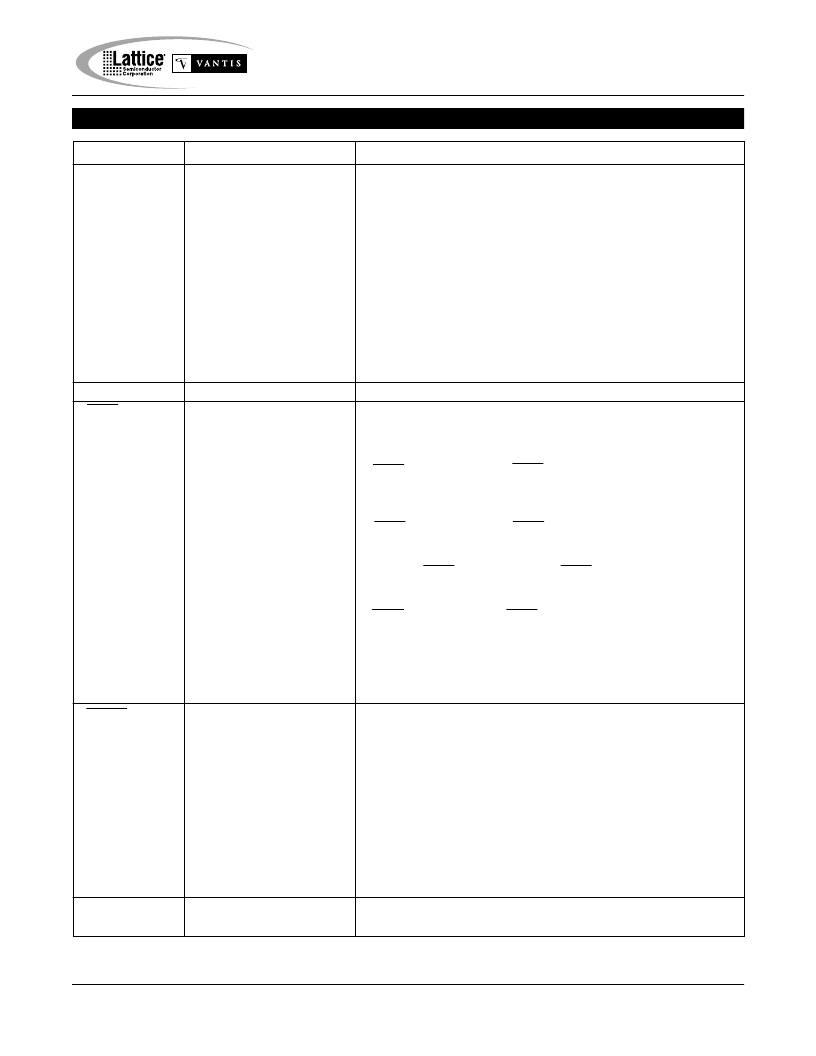
Pin Description
Input
—
Dedicated in-system programming enable input pin. This pin
is brought low to enable the programming mode. The MODE, SDI,
SDO and SCLK options become active.
Input
—
his pin performs two functions. It is a dedicated input pin when
ispEN is logic high. When ispEN is logic low, it functions as an input
pin to load programming data into the device. SDI/IN 0 also is used as
one of the two control pins for the isp state machine.
Input
—
his pin performs two functions. It is a dedicated input pin when
ispEN is logic high. When ispEN is logic low, it functions as a pin to
control the operation of the isp state machine.
Input/Output
—
his pin performs two functions. It is a dedicated input
pin when ispEN is logic high. When ispEN is logic low, it functions as
an output pin to read serial shift register data.
Input
—
his pin performs two functions. It is a dedicated input when
ispEN is logic high. When ispEN is logic low, it functions as a clock pin
for the Serial Shift Register.
No Connect
Description
TQFP Pin Numbers
17,
18,
21,
22,
29,
30,
33,
34,
40,
41,
44,
45,
48,
53,
56,
57,
67,
68,
71,
72,
79,
80,
83,
84,
90,
91,
94,
95,
98,
3,
6,
7,
66,
87,
Name
I/O 0 - I/O 3
I/O 4 - I/O 7
I/O 8 - I/O 11
I/O 12 - I/O 15
I/O 16 - I/O 19
I/O 20 - I/O 23
I/O 24 - I/O 27
I/O 28 - I/O 31
I/O 32 - I/O 35
I/O 36 - I/O 39
I/O 40 - I/O 43
I/O 44 - I/O 47
I/O 48 - I/O 51
I/O 52 - I/O 55
I/O 56 - I/O 59
I/O 60 - I/O 63
IN 4 - IN 7
Input/Output Pins - These are the general purpose I/O pins used by the
logic array.
19,
23,
31,
35,
42,
46,
54,
58,
69,
73,
81,
85,
92,
96,
4,
8,
89,
20,
28,
32,
36,
43,
47,
55,
59,
70,
78,
82,
86,
93,
97,
5,
9
10
Dedicated input pins to the device.
ispEN
14
SDI/IN 0
1
16
MODE/IN 1
1
37
SDO/IN 2
1
39
SCLK/IN 3
1
60
NC
2
1,
26,
51,
76,
2,
27,
52,
77,
24,
49,
74,
99,
25,
50,
75
100
Active Low (0) Reset pin which resets all of the GLB and I/O registers
in the device.
Dedicated Clock input. This clock input is connected to one of the
clock inputs of all of the GLBs on the device.
Dedicated Clock input. This clock input is brought into the clock
distribution network, and can optionally be routed to any GLB on the
device.
Dedicated Clock input. This clock input is brought into the clock
distribution network, and can optionally be routed to any GLB and/or
any I/O cell on the device.
Dedicated Clock input. This clock input is brought into the clock
distribution network, and can optionally be routed to any I/O cell on the
device.
Ground (GND)
V
CC
RESET
15
Y0
11
Y1
65
Y2
62
Y3
61
GND
V
CC
13,
12,
38,
64
63,
88
1. Pins have dual function capability
2. NC pins are not to be connected to any active signals, Vcc or GND.
相關(guān)PDF資料 |
PDF描述 |
|---|---|
| ISPLSI1032-90LJ | In-System Programmable High Density PLD |
| ISPLSI1032-90LT | In-System Programmable High Density PLD |
| ISPLSI1032E-100LJ | In-System Programmable High Density PLD |
| ISPLSI1032E-80LJ | In-System Programmable High Density PLD |
| ISPLSI1032E-80LJ | High-Density Programmable Logic |
相關(guān)代理商/技術(shù)參數(shù) |
參數(shù)描述 |
|---|---|
| ISPLSI1032-80LT/833 | 制造商:LATTICE 制造商全稱(chēng):Lattice Semiconductor 功能描述:In-System Programmable High Density PLD |
| ISPLSI1032-80LTI | 制造商:LATTICE 制造商全稱(chēng):Lattice Semiconductor 功能描述:In-System Programmable High Density PLD |
| ISPLSI1032-90 | 制造商:LATTICE 制造商全稱(chēng):Lattice Semiconductor 功能描述:In-System Programmable High Density PLD |
| ISPLSI1032-90LG | 制造商:LATTICE 制造商全稱(chēng):Lattice Semiconductor 功能描述:In-System Programmable High Density PLD |
| ISPLSI1032-90LG/833 | 制造商:LATTICE 制造商全稱(chēng):Lattice Semiconductor 功能描述:In-System Programmable High Density PLD |
發(fā)布緊急采購(gòu),3分鐘左右您將得到回復(fù)。