- 您現(xiàn)在的位置:買賣IC網(wǎng) > PDF目錄1929 > ISPLSI 1032E-125LJN (Lattice Semiconductor Corporation)IC PLD ISP 64I/O 7.5NS 84PLCC PDF資料下載
參數(shù)資料
| 型號: | ISPLSI 1032E-125LJN |
| 廠商: | Lattice Semiconductor Corporation |
| 文件頁數(shù): | 5/17頁 |
| 文件大小: | 0K |
| 描述: | IC PLD ISP 64I/O 7.5NS 84PLCC |
| 標(biāo)準(zhǔn)包裝: | 15 |
| 系列: | ispLSI® 1000E |
| 可編程類型: | 系統(tǒng)內(nèi)可編程 |
| 最大延遲時(shí)間 tpd(1): | 7.5ns |
| 電壓電源 - 內(nèi)部: | 4.75 V ~ 5.25 V |
| 邏輯元件/邏輯塊數(shù)目: | 32 |
| 門數(shù): | 6000 |
| 輸入/輸出數(shù): | 64 |
| 工作溫度: | 0°C ~ 70°C |
| 安裝類型: | 表面貼裝 |
| 封裝/外殼: | 84-LCC(J 形引線) |
| 供應(yīng)商設(shè)備封裝: | 84-PLCC(29.31x29.31) |
| 包裝: | 管件 |
| 其它名稱: | ISPLSI1032E-125LJN |
13
Specifications ispLSI 1032E
USE
ispLSI
1032EA
FOR
NEW
DESIGNS
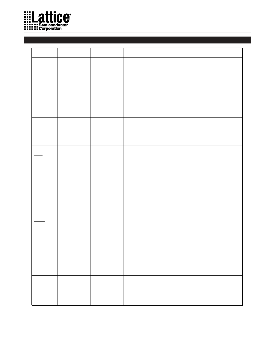
Pin Description
Input - This pin performs two functions. When
ispEN is logic low, it functions
as pin to control the operation of the isp state machine. It is a dedicated
input pin when
ispEN is logic high.
This is a dual function pin. It can be used either as Global Output Enable for
all I/O cells or it can be used as a dedicated input pin.
This is a dual function pin. It can be used either as Global Output Enable for
all I/O cells or it can be used as a dedicated input pin.
Dedicated Clock input. This clock input is brought into the clock distribution
network, and can optionally be routed to any GLB on the device.
Dedicated Clock input. This clock input is connected to one of the clock
inputs of all of the GLBs on the device.
Input/Output Pins - These are the general purpose I/O pins used by the logic
array.
NAME
Table 2-0002A/1032E
PLCC PIN
NUMBERS
DESCRIPTION
26,
30,
34,
38,
45,
49,
53,
57,
68,
72,
76,
80,
3,
7,
11,
15,
27,
31,
35,
39,
46,
50,
54,
58,
69,
73,
77,
81,
4,
8,
12,
16,
28,
32,
36,
40,
47,
51,
55,
59,
70,
74,
78,
82,
5,
9,
13,
17,
I/O 0 - I/O 3
I/O 4 - I/O 7
I/O 8 - I/O 11
I/O 12 - I/O 15
I/O 16 - I/O 19
I/O 20 - I/O 23
I/O 24 - I/O 27
I/O 28 - I/O 31
I/O 32 - I/O 35
I/O 36 - I/O 39
I/O 40 - I/O 43
I/O 44 - I/O 47
I/O 48 - I/O 51
I/O 52 - I/O 55
I/O 56 - I/O 59
I/O 60 - I/O 63
29,
33,
37,
41,
48,
52,
56,
60,
71,
75,
79,
83,
6,
10,
14,
18
66
Y1
20
Y0
42
MODE/IN 12
Ground (GND)
GND
Vcc
VCC
21, 65
NC1
GOE 0/IN 43
Dedicated input pins to the device.
IN 6, IN 7
GOE 1/IN 53
2,
84
67
19
Input - Dedicated in-system programming enable input pin. This pin is
brought low to enable the programming mode. The MODE, SDI, SDO and
SCLK options become active.
23
ispEN
Input - This pin performs two functions. When
ispEN is logic low, it functions
as an input pin to load programming data into the device. SDI/IN 0 is also
used as one of the two control pins for the isp state machine. It is a
dedicated input pin when
ispEN is logic high.
25
SDI/IN 02
44
SDO/IN 22
Output/Input - This pin performs two functions. When
ispEN is logic low, it
functions as an output pin to read serial shift register data. It is a dedicated
input pin when
ispEN is logic high.
61
SCLK/IN 32
Input - This pin performs two functions. When
ispEN is logic low, it functions
as a clock pin for the Serial Shift Register. It is a dedicated input pin when
ispEN is logic high.
Active Low (0) Reset pin which resets all of the GLB and I/O registers in the
device.
24
RESET
Dedicated Clock input. This clock input is brought into the clock distribution
network, and can optionally be routed to any GLB and/or any I/O cell on the
device.
63
Y2
Dedicated Clock input. This clock input is brought into the clock distribution
network, and can optionally be routed to any I/O cell on the device.
62
Y3
1,
22,
43,
64
12,
1,
26,
51,
76,
64
2,
24, 25,
No connect.
27,
49, 50,
52,
74, 75,
77,
99, 100
1. NC pins are not to be connected to any active signals, Vcc or GND.
2. Pins have dual function capability.
3. Pins have dual function capability which is software selectable.
TQFP PIN
NUMBERS
17,
21,
29,
33,
40,
44,
48,
56,
67,
71,
79,
83,
90,
94,
98,
6,
18,
22,
30,
34,
41,
45,
53,
57,
68,
72,
80,
84,
91,
95,
3,
7,
19,
23,
31,
35,
42,
46,
54,
58,
69,
73,
81,
85,
92,
96,
4,
8,
20,
28,
32,
36,
43,
47,
55,
59,
70,
78,
82,
86,
93,
97,
5,
9
65
11
37
89,
87
66
10
14
16
39
60
15
62
61
13, 38,
63,
88
相關(guān)PDF資料 |
PDF描述 |
|---|---|
| ISPLSI 1032EA-200LT100 | IC PLD ISP 64I/O 4.5NS 100TQFP |
| ISPLSI 1048-50LQI | IC PLD ISP 96I/O 18NS 120PQFP |
| ISPLSI 1048C-50LQI | IC PLD ISP 96I/O 22NS 128PQFP |
| ISPLSI 1048E-125LTN | IC PLD ISP 96I/O 7.5NS 128TQFP |
| ISPLSI 1048EA-170LT128 | IC PLD ISP 96I/O 5NS 128TQFP |
相關(guān)代理商/技術(shù)參數(shù) |
參數(shù)描述 |
|---|---|
| ispLSI1032E-125LJN | 功能描述:CPLD - 復(fù)雜可編程邏輯器件 USE ispMACH 4000V RoHS:否 制造商:Lattice 系列: 存儲(chǔ)類型:EEPROM 大電池?cái)?shù)量:128 最大工作頻率:333 MHz 延遲時(shí)間:2.7 ns 可編程輸入/輸出端數(shù)量:64 工作電源電壓:3.3 V 最大工作溫度:+ 90 C 最小工作溫度:0 C 封裝 / 箱體:TQFP-100 |
| ISPLSI1032E125LJNI | 制造商:LATTICE 制造商全稱:Lattice Semiconductor 功能描述:In-System Programmable High Density PLD |
| ISPLSI1032E125LT | 制造商:LATT 功能描述: |
| ispLSI1032E-125LT | 功能描述:CPLD - 復(fù)雜可編程邏輯器件 USE ispMACH 4000V RoHS:否 制造商:Lattice 系列: 存儲(chǔ)類型:EEPROM 大電池?cái)?shù)量:128 最大工作頻率:333 MHz 延遲時(shí)間:2.7 ns 可編程輸入/輸出端數(shù)量:64 工作電源電壓:3.3 V 最大工作溫度:+ 90 C 最小工作溫度:0 C 封裝 / 箱體:TQFP-100 |
| ISPLSI1032E125LTI | 制造商:LATTICE 制造商全稱:Lattice Semiconductor 功能描述:In-System Programmable High Density PLD |
發(fā)布緊急采購,3分鐘左右您將得到回復(fù)。