- 您現(xiàn)在的位置:買賣IC網(wǎng) > PDF目錄360997 > ISO165 Precision Instrumentation Amplifier PDF資料下載
參數(shù)資料
| 型號: | ISO165 |
| 元件分類: | 測量放大器 |
| 英文描述: | Precision Instrumentation Amplifier |
| 中文描述: | 精密儀表放大器 |
| 文件頁數(shù): | 3/8頁 |
| 文件大小: | 164K |
| 代理商: | ISO165 |
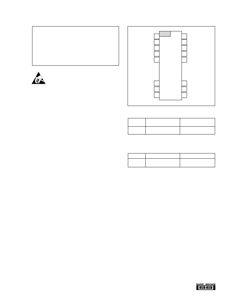
3
ISO165/ISO175
PIN CONFIGURATION
Any integrated circuit can be damaged by ESD. Burr-Brown
recommends that all integrated circuits be handled with
appropriate precautions. Failure to observe proper handling
and installation procedures can cause damage.
ESD damage can range from subtle performance degrada-
tion to complete device failure. Precision integrated circuits
may be more susceptible to damage because very small
parametric changes could cause the device not to meet
published specifications.
PACKAGE INFORMATION
PACKAGE DRAWING
NUMBER
(1)
MODEL
PACKAGE
ISO165P
ISO175P
24-Pin Plastic DIP
24-Pin Plastic DIP
243-2
243-2
NOTE: (1) For detailed drawing and dimension table, please see end of data
sheet, or Appendix D of Burr-Brown IC Data Book.
ELECTROSTATIC
DISCHARGE SENSITIVITY
ABSOLUTE MAXIMUM RATINGS
Supply Voltage ...................................................................................
±
18V
Analog Input Voltage Range ..............................................................
±
40V
External Oscillator Input .....................................................................
±
25V
Com 1 to GND1 ...................................................................................
±
1V
Com 2 to GND2 ...................................................................................
±
1V
Continuous Isolation Voltage: ....................................................1500Vrms
IMV, dv/dt...................................................................................... 20kV/
μ
s
Junction Temperature ...................................................................... 150
°
C
Storage Temperature ...................................................... –40
°
C to +125
°
C
Lead Temperature (soldering, 10s)................................................ +300
°
C
Output Short Duration .......................................... Continuous to Common
ORDERING INFORMATION
MODEL
PACKAGE
BANDWIDTH
ISO165P
ISO175P
24-Pin Plastic DIP
24-Pin Plastic DIP
6kHz
60kHz
The information provided herein is believed to be reliable; however, BURR-BROWN assumes no responsibility for inaccuracies or omissions. BURR-BROWN assumes
no responsibility for the use of this information, and all use of such information shall be entirely at the user's own risk. Prices and specifications are subject to change
without notice. No patent rights or licenses to any of the circuits described herein are implied or granted to any third party. BURR-BROWN does not authorize or warrant
any BURR-BROWN product for use in life support devices and/or systems.
V
S1–
V
S1+
Shield 1
Com 2
V
OUT
GND 2
FBP
EXT OSC
GND 1
V
S2+
Shield 2
V
S2–
FBN
Com 1
V
IN–
1
2
3
4
5
10
11
12
24
23
22
21
20
15
14
13
V
IN+
相關(guān)PDF資料 |
PDF描述 |
|---|---|
| ISO166P | Precision, Isolated OPERATIONAL AMPLIFIER |
| ISO166 | |
| ISO175P | Single Supply, Rail-to-Rail, Low Cost Instrumentation Amplifier |
| ISO175 | Single Supply, Rail-to-Rail, Low Cost Instrumentation Amplifier |
| ISO176P | Precision, Isolated OPERATIONAL AMPLIFIER |
相關(guān)代理商/技術(shù)參數(shù) |
參數(shù)描述 |
|---|---|
| ISO165/ISO175 | 制造商:未知廠家 制造商全稱:未知廠家 功能描述:ISO165. ISO175 - DISCONTINUED PRODUCT. No longer recommended for new design. |
| ISO166 | 制造商:未知廠家 制造商全稱:未知廠家 功能描述: |
| ISO166/ISO176 | 制造商:未知廠家 制造商全稱:未知廠家 功能描述:ISO166. ISO176 - DISCONTINUED PRODUCT. No longer recommended for new design. |
| ISO166P | 制造商:BB 制造商全稱:BB 功能描述:Precision, Isolated OPERATIONAL AMPLIFIER |
| ISO16-GM-391 | 功能描述:繼電器插座與硬件 RELAY ISO x16 GADGETEER MODULE RoHS:否 制造商:TE Connectivity / Schrack 附件類型:Socket 相關(guān)繼電器系列:RP, RT, RY 端接類型:PCB 極數(shù):1 |
發(fā)布緊急采購,3分鐘左右您將得到回復(fù)。