- 您現(xiàn)在的位置:買(mǎi)賣(mài)IC網(wǎng) > PDF目錄384510 > IRS21366 (International Rectifier) 3-PHASE BRIDGE DRIVER PDF資料下載
參數(shù)資料
| 型號(hào): | IRS21366 |
| 廠商: | International Rectifier |
| 英文描述: | 3-PHASE BRIDGE DRIVER |
| 中文描述: | 3相橋式驅(qū)動(dòng)器 |
| 文件頁(yè)數(shù): | 5/23頁(yè) |
| 文件大小: | 614K |
| 代理商: | IRS21366 |
第1頁(yè)第2頁(yè)第3頁(yè)第4頁(yè)當(dāng)前第5頁(yè)第6頁(yè)第7頁(yè)第8頁(yè)第9頁(yè)第10頁(yè)第11頁(yè)第12頁(yè)第13頁(yè)第14頁(yè)第15頁(yè)第16頁(yè)第17頁(yè)第18頁(yè)第19頁(yè)第20頁(yè)第21頁(yè)第22頁(yè)第23頁(yè)
www.irf.com
5
IRS213(6,62,63,65,66,67,68) (J&S)PbF
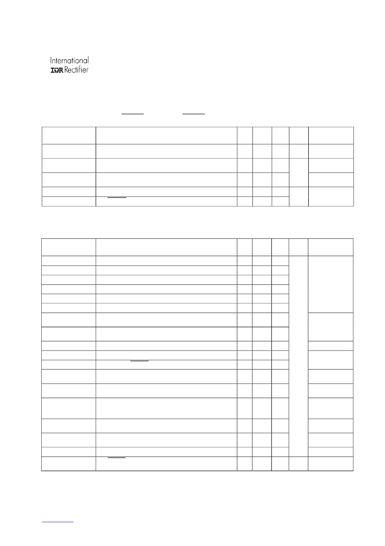
Static Electrical Characteristics - (Continued)
V
BIAS
(V
CC
,V
BS1,2,3
) = 15 V unless otherwise specified. The V
IN
, V
TH
, and I
IN
parameters are referenced to V
SS
and are
applicable to all six channels (HIN1,2,3/HIN1,2,3 and LIN1,2,3). The V
O
and I
O
parameters are referenced to COM and
V
S1,2,3
and are applicable to the respective output leads: LO1,2,3 and HO1,2,3.
Symbol
Definition
Min. Typ. Max. Units
Test
Conditions
V
RCIN
= 0 V or
15 V
Vo =0 V,
PW
≤
10 μs
Vo =15 V,
PW
≤
10 μs
I
RCIN
RCIN input bias current
—
—
1
μA
I
O+
Output high short circuit pulsed current
120
200
—
I
O-
Output low short circuit pulsed current
250
350
—
mA
R
on_RCIN
R
on_FAULT
RCIN low on resistance
FAULT low on resistance
—
50
100
—
50
100
I= 1.5 mA
Dynamic Electrical Characteristics
Dynamic Electrical Characteristics V
CC
= V
BS
= V
BIAS
= 15 V, V
S1,2,3
= V
SS
= COM, T
A
= 25 °C and CL = 1000 pF unless
otherwise specified.
Symbol
Definition
Min. Typ. Max. Units
Test
Conditions
t
on
t
off
Turn-on propagation delay
400
530
750
Turn-off propagation delay
Turn-on propagation delay
Turn-off propagation delay
Turn-on rise time
Turn-off fall time
ENABLE low to output shutdown propagation
delay
ENABLE low to output shutdown propagation
delay
ITRIP to output shutdown propagation delay
ITRIP blanking time
ITRIP to FAULT propagation delay
Input filter time (HIN, LIN)
(IRS213(6,62,63,65,68) only)
Enable input filter time
(IRS213(6,62,63,65,68) only)
400
—
—
—
—
530
200
200
125
50
750
—
—
190
75
t
on
(66,67)
t
off
(66,67)
t
r
t
f
V
IN
= 0 V & 5 V
t
EN
350
460
650
t
EN
(66,67)
—
300
—
V
IN,
V
EN
= 0 V
or 5 V
t
ITRIP
t
bl
t
FLT
500
—
400
750
400
600
1200
—
950
V
ITRIP
=5 V
V
IN
= 0 V or 5 V
V
ITRIP
= 5 V
t
FILIN
200
350
510
V
IN
= 0 V & 5 V
t
filterEN
100
200
—
DT
Deadtime
190
290
420
V
IN
= 0 V & 5 V
external dead
time
External dead
time >420 ns
External dead
time 0 s
PW input=10 μs
V
IN
= 0 V or 5 V
V
ITRIP
= 0 V
MT
t
on
, t
off
matching time (on all six channels)
—
—
50
MDT
DT matching (Hi->Lo & Lo->Hi on all channels)
—
—
60
PM
Pulse width distortion (pwin-pwout)
FAULT clear time RCIN: R = 2 M
, C = 1 nF
—
—
75
ns
t
FLTCLR
1.3
1.65
2
ms
Note:
For high side PWM, HIN pulse width must be
≥
500 ns.
PRELIMINARY
相關(guān)PDF資料 |
PDF描述 |
|---|---|
| IRS21367 | 3-PHASE BRIDGE DRIVER |
| IRS21368JPbF | 3-PHASE BRIDGE DRIVER |
| IRS21368SPbF | 3-PHASE BRIDGE DRIVER |
| IRS2153D | SELF-OSCILLATING HALF-BRIDEGE DRIVER IC |
| IRS2153DPBF | SELF-OSCILLATING HALF-BRIDEGE DRIVER IC |
相關(guān)代理商/技術(shù)參數(shù) |
參數(shù)描述 |
|---|---|
| IRS21366D | 制造商:IRF 制造商全稱(chēng):International Rectifier 功能描述:3-PHASE BRIDGE DRIVER |
| IRS21367 | 制造商:IRF 制造商全稱(chēng):International Rectifier 功能描述:3-PHASE BRIDGE DRIVER |
| IRS21367D | 制造商:IRF 制造商全稱(chēng):International Rectifier 功能描述:3-PHASE BRIDGE DRIVER |
| IRS21368DJPBF | 制造商:IRF 制造商全稱(chēng):International Rectifier 功能描述:3-PHASE BRIDGE DRIVER |
| IRS21368DSPBF | 制造商:IRF 制造商全稱(chēng):International Rectifier 功能描述:3-PHASE BRIDGE DRIVER |
發(fā)布緊急采購(gòu),3分鐘左右您將得到回復(fù)。