- 您現(xiàn)在的位置:買賣IC網(wǎng) > PDF目錄383107 > ILX503 (Sony Corporation) 2048-pixel CCD Linear Image Sensor (B/W) PDF資料下載
參數(shù)資料
| 型號: | ILX503 |
| 廠商: | Sony Corporation |
| 英文描述: | 2048-pixel CCD Linear Image Sensor (B/W) |
| 中文描述: | 2048像素CCD線性圖像傳感器(黑/白) |
| 文件頁數(shù): | 3/15頁 |
| 文件大小: | 198K |
| 代理商: | ILX503 |
– 3 –
ILX503A
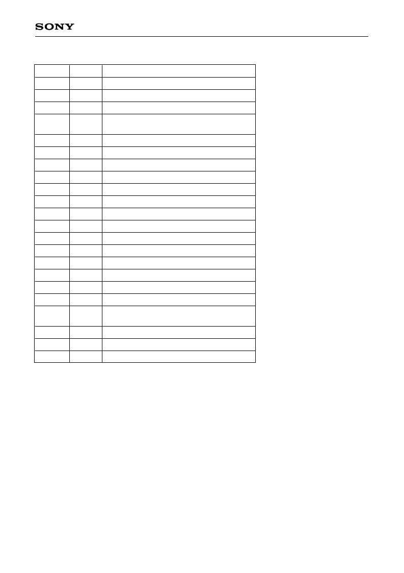
Pin Description
Pin No.
1
2
3
4
5
6
7
8
9
10
11
12
13
14
15
16
17
18
19
20
21
22
Symbol
V
OUT
GND
GND
SHSW
φ
CLK
V
DD1
GND
V
DD2
T1
NC
φ
ROG
GND
NC
NC
V
DD1
GND
GND
V
GG
RSSW
V
DD1
EXRS
V
DD2
Description
Signal output
GND
GND
with S/H
→
GND
without S/H
→
V
DD2
Switch
Clock pulse
9V power supply
GND
5V power supply
Test pin (V
DD2
)
Clock pulse
GND
9V power supply
GND
GND
Output circuit gate bias
RS pulse external, internal selection
(External RS
→
V
DD2
, Internal RS
→
GND)
9V power supply
RS input pin during external RS pulse usage
5V power supply
{
發(fā)布緊急采購,3分鐘左右您將得到回復。