- 您現(xiàn)在的位置:買賣IC網(wǎng) > PDF目錄360754 > ICS664-02 PECL Digital Video Clock Source PDF資料下載
參數(shù)資料
| 型號: | ICS664-02 |
| 英文描述: | PECL Digital Video Clock Source |
| 中文描述: | PECL的數(shù)字視頻時鐘源 |
| 文件頁數(shù): | 2/6頁 |
| 文件大?。?/td> | 97K |
| 代理商: | ICS664-02 |
PECL Digital Video Clock Source
MDS 664-02 C
2
Revision 062304
Integrated Circuit Systems, Inc.
●
525 Race Street, San Jose, CA 95126
●
tel (408) 297-1201
●
www.icst.com
ICS664-02
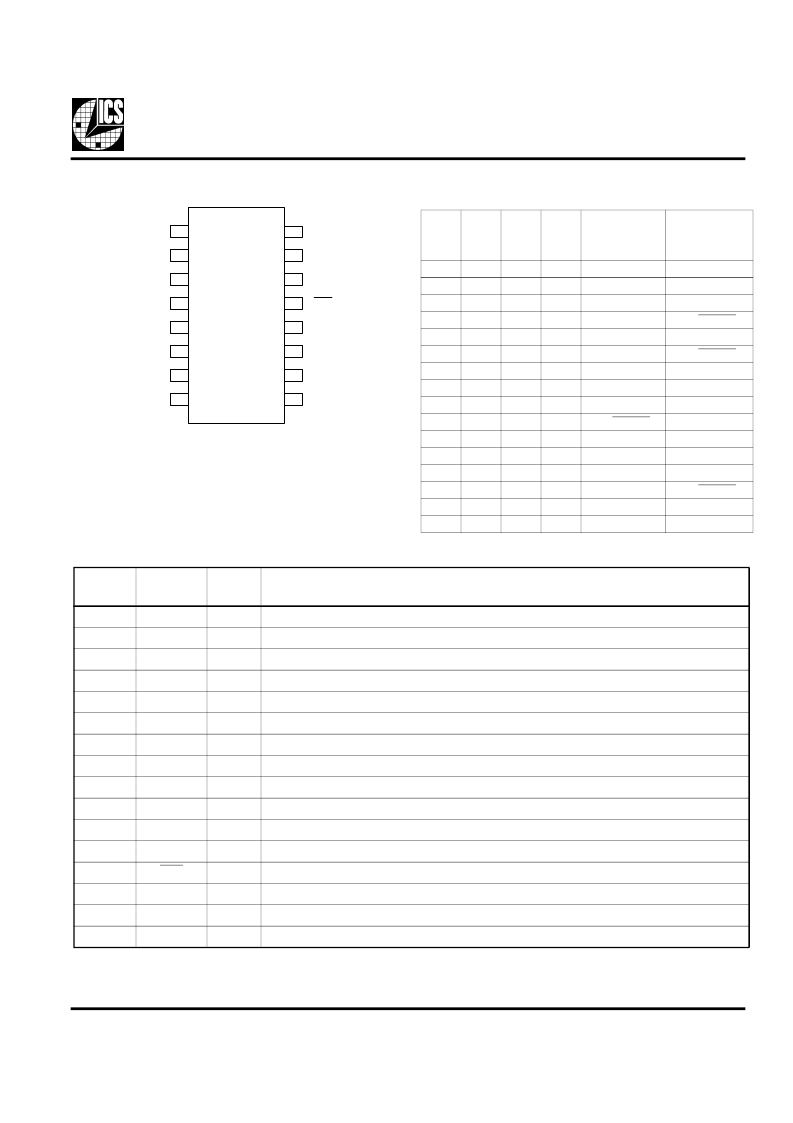
Pin Assignment
16-pin 4.40 mil body, 0.65 mm pitch TSSOP
Output Clock Selection Table
Pin Descriptions
12
1
11
2
10
X1/REFIN
X2
3
9
VDD
4
VDD
VDDO
5
S0
6
CLK
7
GND
8
GND
CLK
GND
SELIN
S3
VDD
S2
S1
16
15
14
13
S3
S2
S1
S0
Input
Frequency
(MHz)
Output
Frequency
(MHz)
0
0
0
0
0
0
0
0
1
1
1
1
1
1
1
1
0
0
0
0
1
1
1
1
0
0
0
0
1
1
1
1
0
0
1
1
0
0
1
1
0
0
1
1
0
0
1
1
0
1
0
1
0
1
0
1
0
1
0
1
0
1
0
1
Power down
Input Freq
74.25
74.175824
74.25
74.175824
RESERVED
RESERVED
54
54
RESERVED
RESERVED
74.25
74.175824
13.5
13.5
Pass thru
27
27
13.5
13.5
RESERVED
RESERVED
74.25
74.175824
RESERVED
RESERVED
54
54
54
27
Pin
Number
Pin
Name
Pin
Type
Pin Description
1
X1/REFIN
Input
Connect this pin to a crystal or clock input
2
VDD
Power
Power supply for crystal oscillator.
3
VDD
Power
Power supply for PLL.
4
S0
Input
Output frequency selection. Determines output frequency per table above. On chip pull-up.
5
GND
Power
Ground for PLL.
6
GND
Power
Ground for oscillator.
7
S3
Input
Output frequency selection. Determines output frequency per table above. On chip pull-up.
8
S2
Input
Output frequency selection. Determines output frequency per table above. On chip pull-up.
9
S1
Input
Output frequency selection. Determines output frequency per table above. On chip pull-up.
10
VDD
Power
Power supply.
11
SELIN
Input
Low for clock input, high for crystal. On chip pull-up.
12
GND
Power
Ground for output stage
13
CLK
Output
Complimentary clock output.
14
CLK
Output
Clock output.
15
VDDO
Power
Power supply for output stage.
16
X2
Input
Connect this pin to a crystal. Leave open if using a clock input.
相關(guān)PDF資料 |
PDF描述 |
|---|---|
| ICS664G-02TR | PECL Digital Video Clock Source |
| ICS664G-02 | PECL Digital Video Clock Source |
| ICS664G-02LF | PECL Digital Video Clock Source |
| ICS664G-02LFTR | PECL Digital Video Clock Source |
| ICS664-03 | Digital Video Clock Source |
相關(guān)代理商/技術(shù)參數(shù) |
參數(shù)描述 |
|---|---|
| ICS664-03 | 制造商:ICS 制造商全稱:ICS 功能描述:Digital Video Clock Source |
| ICS664-03LF | 制造商:ICS 制造商全稱:ICS 功能描述:Digital Video Clock Source |
| ICS664-03LFT | 制造商:ICS 制造商全稱:ICS 功能描述:Digital Video Clock Source |
| ICS664-03T | 制造商:ICS 制造商全稱:ICS 功能描述:Digital Video Clock Source |
| ICS664-04 | 制造商:ICS 制造商全稱:ICS 功能描述:PECL Digital Video Clock Source |
發(fā)布緊急采購,3分鐘左右您將得到回復(fù)。