- 您現(xiàn)在的位置:買賣IC網(wǎng) > PDF目錄360752 > ICS650-27 Networking Clock Source PDF資料下載
參數(shù)資料
| 型號: | ICS650-27 |
| 英文描述: | Networking Clock Source |
| 中文描述: | 網(wǎng)絡(luò)時鐘源 |
| 文件頁數(shù): | 1/6頁 |
| 文件大小: | 99K |
| 代理商: | ICS650-27 |
ICS650-27
MDS 650-27 D
1
Revision 070505
Integrated Circuit Systems, Inc.
●
525 Race Street, San Jose, CA 95126
●
tel (408) 297-1201
●
www.icst.com
Networking Clock Source
Description
The ICS650-27 is a low cost, low jitter, high
performance clock synthesizer for networking
applications. Using analog Phase-Locked Loop (PLL)
techniques, the device accepts a 12.5 MHz or 25 MHz
clock or fundamental mode crystal input to produce
multiple output clocks for networking chips, PCI
devices, SDRAM, and ASICs. The ICS650-27 outputs
all have zero ppm synthesis error.
The ICS650-27 is pin compatible and functionally
equivalent to the ICS650-07. It is a performance
upgrade and is recommended for all new 3.3V
designs.
See the MK74CB214, ICS551, and ICS552-01 for
non-PLL buffer devices which produce multiple
low-skew copies of these output clocks.
See the ICS570, ICS9112-16/17/18 for zero delay
buffers that can synchronize outputs and other needed
clocks.
Features
Packaged in 20-pin (150 mil) SSOP (QSOP)
Available in Pb (lead) free package
12.5 MHz or 25 MHz fundamental crystal or clock
input
Six output clocks with selectable frequencies
SDRAM frequencies of 67, 83, 100, and 133 MHz
Buffered crystal reference output
Zero ppm synthesis error in all clocks
Ideal for PMC-Sierra’s ATM switch chips
Full CMOS output swing with 25 mA output drive
capability at TTL levels
Advanced, low-power, sub-micron CMOS process
Operating voltage of 3.3 V
Industrial temperature only
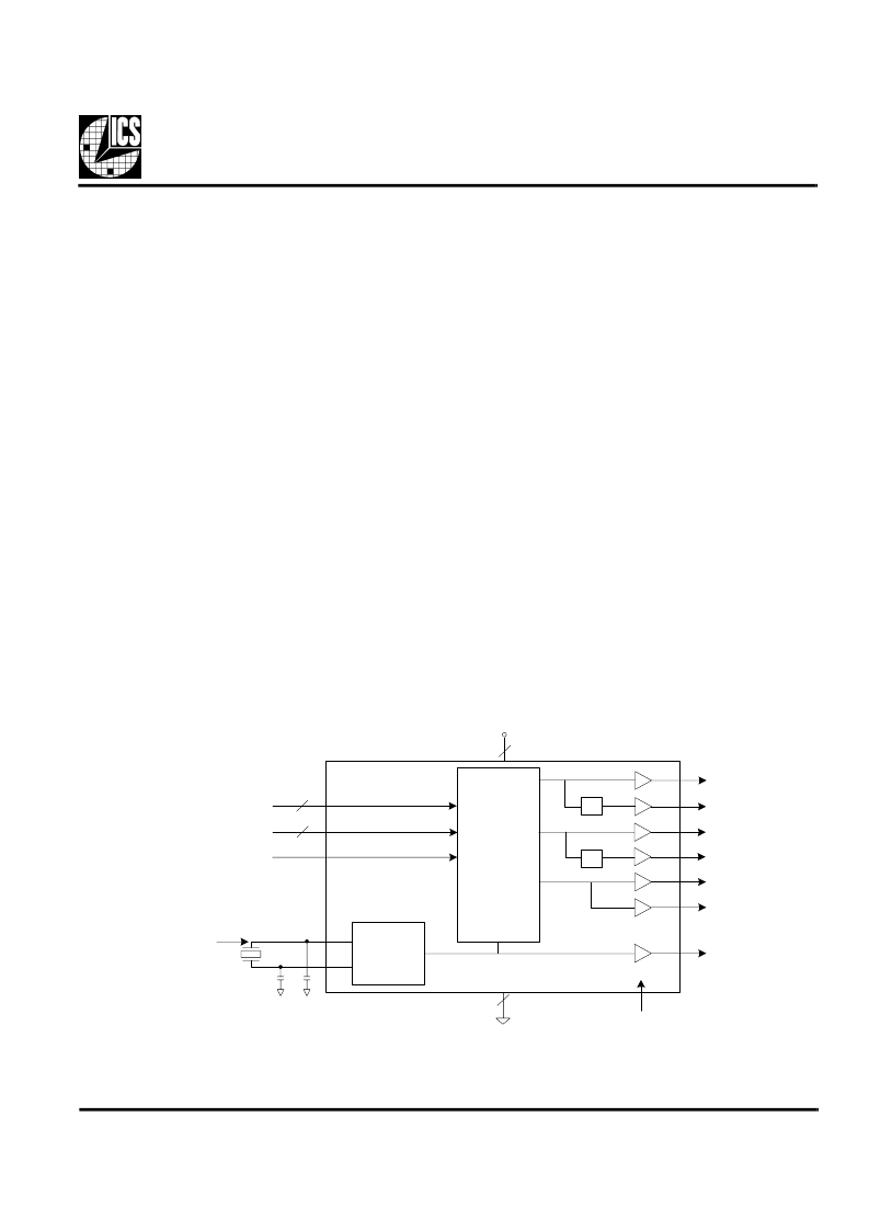
Block Diagram
Clock
Buffer/
Crystal
Oscillator
Clock
Synthesis
and Control
Circuitry
25 or 12.5 MHz
cyrstal or clock
ACS1:0
CLKA1
CCS
GND
2
BCS1:0
2
2
X1/ICLK
X2
CLKA2
CLKB1
CLKB2
CLKC1
CLKC2
REFOUT
VDD
2
/2
/2
OE (all outputs)
相關(guān)PDF資料 |
PDF描述 |
|---|---|
| ICS650R-27I | Networking Clock Source |
| ICS650R-27ILF | Networking Clock Source |
| ICS650R-27ILFT | Networking Clock Source |
| ICS650R-27IT | Networking Clock Source |
| ICS650-36 | Networking & PCI Clock Source |
相關(guān)代理商/技術(shù)參數(shù) |
參數(shù)描述 |
|---|---|
| ICS650-36 | 制造商:ICS 制造商全稱:ICS 功能描述:Networking & PCI Clock Source |
| ICS650-40 | 制造商:ICS 制造商全稱:ICS 功能描述:ETHERNET SWITCH CLOCK SOURCE |
| ICS650-40A | 制造商:ICS 制造商全稱:ICS 功能描述:ETHERNET SWITCH CLOCK SOURCE |
| ICS650-41 | 制造商:ICS 制造商全稱:ICS 功能描述:Spread Spectrum Clock Synthesizer |
| ICS650-44 | 制造商:ICS 制造商全稱:ICS 功能描述:Spread Spectrum Clock Synthesizer |
發(fā)布緊急采購,3分鐘左右您將得到回復(fù)。