- 您現(xiàn)在的位置:買賣IC網(wǎng) > PDF目錄65530 > ICS614M-01T (INTEGRATED DEVICE TECHNOLOGY INC) 48 MHz, VIDEO CLOCK GENERATOR, PDSO16 PDF資料下載
參數(shù)資料
| 型號: | ICS614M-01T |
| 廠商: | INTEGRATED DEVICE TECHNOLOGY INC |
| 元件分類: | 時(shí)鐘產(chǎn)生/分配 |
| 英文描述: | 48 MHz, VIDEO CLOCK GENERATOR, PDSO16 |
| 封裝: | SOIC-16 |
| 文件頁數(shù): | 2/4頁 |
| 文件大小: | 65K |
| 代理商: | ICS614M-01T |
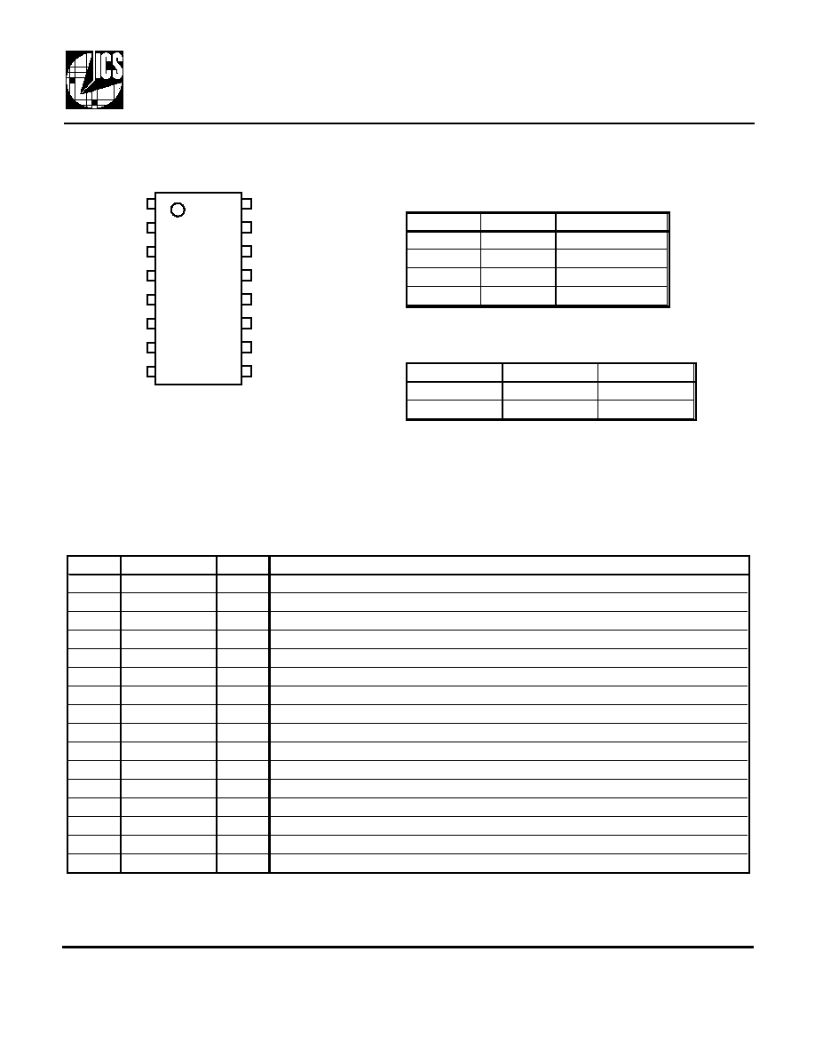
ICS614-01
16 pin Intel Graphics Clock Source
MDS 614-01 B
2
Revision 020199
Printed 11/14/00
Integrated Circuit Systems 525 Race Street San Jose CA95126 (408) 295-9800tel (408) 295-9818fax
I C R O
C LOC K
PRELIMINARY INFORMATION
Pin Descriptions
Key: I = Input; O = output; P = power supply connection; XI, XO = crystal connections.
Pin Assignment
Number
Name
Type
Description
1
OE
I
Output Enable. Tri-states all output clocks when low. All running when high (VDDIO).
2
X2
XO
Crystal connection. Connect to a 27 MHz fundamental parallel mode crystal.
3
X1/ICLK
XI
Crystal connection. Connect to a 27 MHz fundamental parallel mode crystal, or clock
4
VDD
P
Connect to +5V.
5
GND
P
Connect to ground.
6
DSEL
I
Input select. Determines DCLK and DCLK/2 per table above. Must be
≤ VDDIO.
7
27M
O
Buffered crystal oscillator 27 MHz clock output. Amplitude = VDDIO.
8
DCLK/2
O
NTSC or PAL 4X subcarrier frequency per table above. Amplitude = VDDIO.
9
48M
O
48.00 MHz clock output for Intel graphics processor. Amplitude = VDDIO.
10
DCLK
O
NTSC or PAL 8X subcarrier frequency per table above. Amplitude = VDDIO.
11
ACLK
O
Audio clock, or Square Pixel clock, per table above. Amplitude = VDDIO.
12
GND
P
Connect to ground.
13
VDDIO
P
Connect to +5V or +3.3V. Amplitude of output clocks will match this voltage.
14
13.5M
O
Buffered crystal oscillator divided by two 13.5 MHz clock output. Amplitude = VDDIO.
15
ASEL0
I
Input select 0 for ACLK. Determines ACLK frequency per table above. Must be
≤ VDDIO.
16
ASEL1
I
Input select 1 for ACLK. Determines ACLK frequency per table above. Must be
≤ VDDIO.
ICS614-01
All Clock frequencies are in MHz.
0=connect directly to ground
1=connect directly to VDDIO
1
8
9
16
2
3
4
5
6
7
10
11
12
13
14
15
ACLK
13.5M
ASEL0
VDDIO
GND
OE
X2
27M
DSEL
VDD
GND
X1/ICLK
DCLK/2
DCLK
ASEL1
48MHz
ASEL1
ASEL0
ACLK
0
Off
0
1
29.4923 MHz
1
0
24.5454 MHz
1
24.576 MHz
DSEL
DCLK
DCLK/2
0
35.4689
17.73445
1
28.63636
14.31818
DCLK Select Table for NTSC/PAL
ACLK Select Table for Audio and Square Pixel
相關(guān)PDF資料 |
PDF描述 |
|---|---|
| ICS650GI-47LFT | 50 MHz, OTHER CLOCK GENERATOR, PDSO16 |
| ICS650R-12 | 108 MHz, VIDEO CLOCK GENERATOR, PDSO20 |
| ICS650R-14 | 133.33 MHz, OTHER CLOCK GENERATOR, PDSO20 |
| ICS650R-14ILF | 133.33 MHz, OTHER CLOCK GENERATOR, PDSO20 |
| ICS650R-14ILFT | 133.33 MHz, OTHER CLOCK GENERATOR, PDSO20 |
相關(guān)代理商/技術(shù)參數(shù) |
參數(shù)描述 |
|---|---|
| ICS615 | 制造商:ICS 制造商全稱:ICS 功能描述:Set-Top Box Clock Source |
| ICS615M | 制造商:ICS 制造商全稱:ICS 功能描述:Set-Top Box Clock Source |
| ICS615MT | 制造商:ICS 制造商全稱:ICS 功能描述:Set-Top Box Clock Source |
| ICS620-01 | 制造商:ICS 制造商全稱:ICS 功能描述:Digital Still Camera Clock Source |
| ICS620-01R | 制造商:ICS 制造商全稱:ICS 功能描述:Digital Still Camera Clock Source |
發(fā)布緊急采購,3分鐘左右您將得到回復(fù)。