- 您現(xiàn)在的位置:買賣IC網(wǎng) > PDF目錄360707 > IBMN364804CT3C-75A x8 SDRAM PDF資料下載
參數(shù)資料
| 型號(hào): | IBMN364804CT3C-75A |
| 英文描述: | x8 SDRAM |
| 中文描述: | x8 SDRAM內(nèi)存 |
| 文件頁數(shù): | 30/71頁 |
| 文件大?。?/td> | 1251K |
| 代理商: | IBMN364804CT3C-75A |
第1頁第2頁第3頁第4頁第5頁第6頁第7頁第8頁第9頁第10頁第11頁第12頁第13頁第14頁第15頁第16頁第17頁第18頁第19頁第20頁第21頁第22頁第23頁第24頁第25頁第26頁第27頁第28頁第29頁當(dāng)前第30頁第31頁第32頁第33頁第34頁第35頁第36頁第37頁第38頁第39頁第40頁第41頁第42頁第43頁第44頁第45頁第46頁第47頁第48頁第49頁第50頁第51頁第52頁第53頁第54頁第55頁第56頁第57頁第58頁第59頁第60頁第61頁第62頁第63頁第64頁第65頁第66頁第67頁第68頁第69頁第70頁第71頁
IBMN364164
IBMN364404
64Mb Synchronous DRAM - Die Revision C
IBMN364804
IBM Corporation. All rights reserved.
Use is further subject to the provisions at the end of this document.
Page 30 of 71
19L3265.E35856B
1/01
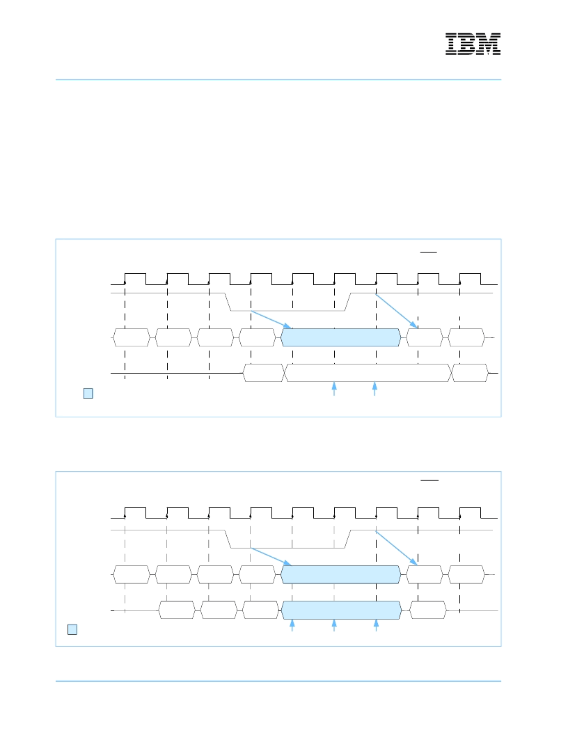
Clock Suspend Mode
During normal access mode, CKE is held high, enabling the clock. When CKE is registered low while at least
one of the banks is active, Clock Suspend Mode is entered. The Clock Suspend mode deactivates the inter-
nal clock and suspends or “freezes” any clocked operation that was currently being executed. There is a one-
clock delay between the registration of CKE low and the time at which the SDRAM’s operation suspends.
While in Clock Suspend mode, the SDRAM ignores any new commands that are issued. The Clock Suspend
mode is exited by bringing CKE high. There is a one clock cycle delay from when CKE returns high to when
Clock Suspend mode is exited.
When the operation of the SDRAM is suspended during the execution of a Burst Read operation, the last
valid data output onto the DQ pins will be actively held valid until Clock Suspend mode is exited.
Clock Suspend during a Read Cycle
If Clock Suspend mode is initiated during a burst write operation, the input data is masked and is ignored until
the Clock Suspend mode is exited.
Clock Suspend during a Write Cycle
CLK
T0
T2
T1
T3
T4
T5
T6
T7
T8
COMMAND
NOP
READ A
NOP
NOP
NOP
NOP
CKE
DQs
DOUT A
0
DOUT A
2
DOUT A
1
: “H” or “L”
A one clock delay before
suspend operation starts
A one clock delay to exit
the Suspend command
DOUT element at the DQs when the
suspend operation starts is held valid
(Burst Length = 4, CAS Latency = 2)
CLK
T0
T2
T1
T3
T4
T5
T6
T7
T8
COMMAND
NOP
WRITE A
NOP
NOP
NOP
NOP
CKE
DQs
DIN A
2
DIN A
3
: “H” or “L”
A one clock delay before
suspend operation starts
A one clock delay to exit
the Suspend command
DIN is masked during the Clock Suspend Period
DIN A
1
DIN A
0
(Burst Length = 4, CAS Latency = 2)
相關(guān)PDF資料 |
PDF描述 |
|---|---|
| IBMSGRF0100 | TRANSISTOR | BJT | NPN | 4.5V V(BR)CEO | 75MA I(C) | SOT-353 |
| IBT200-200 | DC to DC Converter |
| IBT200-201 | DC to DC Converter |
| IBT200-201-3 | DC to DC Converter |
| IBT200-202 | DC to DC Converter |
相關(guān)代理商/技術(shù)參數(shù) |
參數(shù)描述 |
|---|---|
| IBMPPC403GAJC33C1 | 制造商:IBM 功能描述: |
| IBMPPC750CLGEQ4023 | 制造商:IBM 功能描述:MPU 750CL RISC 32BIT 90NM 400MHZ 1.15V/1.8V 278FCBGA - Trays |
| IBMPPC750CLGEQ5023 | 制造商:IBM Microelectronics 功能描述:MPU 750CL RISC 32BIT 90NM 500MHZ 1.15V/1.8V 278FCBGA - Trays |
| IBMPPC750CLGEQA033 | 制造商:IBM 功能描述:MPU 750CL RISC 32BIT 90NM 1GHZ 1.15V/1.8V 278FCBGA - Trays 制造商:IBM 功能描述:IBMIBMPPC750CLGEQA033 CPU PPC 750CL 1GHZ |
| IBN100 | 制造商:Hubbell Wiring Device-Kellems 功能描述:ICON, BLANK,BR,100PK |
發(fā)布緊急采購,3分鐘左右您將得到回復(fù)。