- 您現(xiàn)在的位置:買賣IC網(wǎng) > PDF目錄384452 > HV3418DG (SUPERTEX INC) 64-Channel Serial To Parallel Converter With High Voltage Push-Pull Outputs PDF資料下載
參數(shù)資料
| 型號: | HV3418DG |
| 廠商: | SUPERTEX INC |
| 元件分類: | 外設及接口 |
| 英文描述: | 64-Channel Serial To Parallel Converter With High Voltage Push-Pull Outputs |
| 中文描述: | SIPO BASED PRPHL DRVR, CQFP80 |
| 封裝: | QUAD, CERPAK-80 |
| 文件頁數(shù): | 1/5頁 |
| 文件大小: | 443K |
| 代理商: | HV3418DG |
12/13/01
Supertex Inc. does not recommend the use of its products in life support applications and will not knowingly sell its products for use in such applications unless it receives an adequate "products liability
indemnification insurance agreement." Supertex does not assume responsibility for use of devices described and limits its liability to the replacement of devices determined to be defective due to
workmanship. No responsibility is assumed for possible omissions or inaccuracies. Circuitry and specifications are subject to change without notice. For the latest product specifications, refer to the
Supertex website: http://www.supertex.com. For complete liability information on all Supertex products, refer to the most current databook or to the Legal/Disclaimer page on the Supertex website.
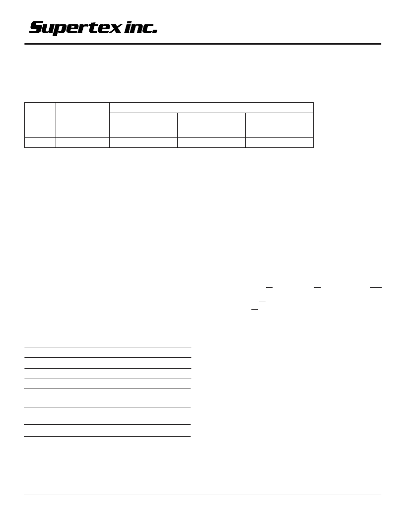
Package Options
Recommended
Operating
V
PP
Max
180V
80-Lead
Quad Cerpak
Gullwing
80-Lead
Quad Plastic
Gullwing
Device
Die
HV3418
HV3418DG
HV3418PG
HV3418X
HV3418
64-Channel Serial To Parallel Converter
With High Voltage Push-Pull Outputs
Ordering Information
General Description
The HV34 is a low voltage serial to high voltage parallel converter
with push-pull outputs. This device has been designed for use as
a printer driver for inkjet applications. It can also be used in any
application requiring multiple output high voltage, low current
sourcing and sinking capabilities.
The device consists of a 64-bit shift register, 64 latches, and
control logic to perform the polarity select and blanking of the
outputs. A DIR pin controls the direction of data shift through the
device. With DIR grounded, D
IOA
is Data-In and D
IOB
is Data-Out;
data is shifted from HV
OUT
64 to HV
OUT
1. When DIR is at logic high,
D
IOB
is Data-In and D
IOA
is Data-Out: data is then shifted from
HV
OUT
1 to HV
OUT
64. Data is shifted through the shift register on
the low to high transition of the clock. Data output buffers are
provided for cascading devices. Operation of the shift register is
not affected by the LE (latch enable), BL (blanking), or the POL
(polarity) inputs. Transfer of data from the shift register to the latch
occurs when the LE (latch enable) is high. The data in the latch is
stored during LE transition from high to low.
Features
HVCMOS
technology
Output voltages up to 180V
Low power level shifting
Shift register speed: 6MHz @ V
DD
= 5V
12MHz @ V
DD
= 12V
Latched data outputs
Output polarity and blanking
CMOS compatible inputs
Forward and reverse shifting options
Absolute Maximum Ratings
1
Supply voltage, V
DD
Supply voltage, V
PP
Logic input levels
-0.5V to +15V
V
DD
to +200V
-0.5V to V
DD
+0.5V
Ground current
2
1.5A
High voltage supply current
2
1.3A
Continuous total power dissipation
3
Ceramic
1900mW
1200mW
Plastic
Operating temperature range
Ceramic -55
°
C to +125
°
C
Plastic
-40
°
C to +85
°
C
Storage temperature range
-65
°
C to +150
°
C
Notes:
1. All voltages are referenced to GND.
2. Connection to all power and ground pads is required. Duty cycle is limited by
the total power dissipated in the package.
3. For operation above 25
°
C ambient derate linearly to maximum operating
temperature at 20mW/
°
C for plastic and at 31.7mW/
°
C for ceramic.
相關PDF資料 |
PDF描述 |
|---|---|
| HV3418PG | 64-Channel Serial To Parallel Converter With High Voltage Push-Pull Outputs |
| HV3418X | 64-Channel Serial To Parallel Converter With High Voltage Push-Pull Outputs |
| HV3418 | 64-Channel Serial To Parallel Converter With High Voltage Push-Pull Outputs |
| HV3418 | 64-Channel Serial To Parallel Converter With High Voltage Push-Pull Outputs(帶高壓推挽輸出的64通道串行到并行轉換器) |
| HV3922 | High Voltage PIN Diode Driver |
相關代理商/技術參數(shù) |
參數(shù)描述 |
|---|---|
| HV3418PG | 功能描述:計數(shù)器移位寄存器 64-Ch Converter RoHS:否 制造商:Texas Instruments 計數(shù)器類型: 計數(shù)順序:Serial to Serial/Parallel 電路數(shù)量:1 封裝 / 箱體:SOIC-20 Wide 邏輯系列: 邏輯類型: 輸入線路數(shù)量:1 輸出類型:Open Drain 傳播延遲時間:650 ns 最大工作溫度:+ 125 C 最小工作溫度:- 40 C 封裝:Reel |
| HV3418PG-G | 功能描述:計數(shù)器移位寄存器 64-Ch Converter RoHS:否 制造商:Texas Instruments 計數(shù)器類型: 計數(shù)順序:Serial to Serial/Parallel 電路數(shù)量:1 封裝 / 箱體:SOIC-20 Wide 邏輯系列: 邏輯類型: 輸入線路數(shù)量:1 輸出類型:Open Drain 傳播延遲時間:650 ns 最大工作溫度:+ 125 C 最小工作溫度:- 40 C 封裝:Reel |
| HV3418T | 制造商:未知廠家 制造商全稱:未知廠家 功能描述:Interface IC |
| HV3418X | 制造商:SUPERTEX 制造商全稱:SUPERTEX 功能描述:64-Channel Serial To Parallel Converter With High Voltage Push-Pull Outputs |
| HV341C | 制造商:未知廠家 制造商全稱:未知廠家 功能描述:Interface IC |
發(fā)布緊急采購,3分鐘左右您將得到回復。