- 您現(xiàn)在的位置:買賣IC網(wǎng) > PDF目錄371900 > HT36A0(48DIP) Microcontroller PDF資料下載
參數(shù)資料
| 型號: | HT36A0(48DIP) |
| 英文描述: | Microcontroller |
| 中文描述: | 微控制器 |
| 文件頁數(shù): | 14/21頁 |
| 文件大小: | 229K |
| 代理商: | HT36A0(48DIP) |
HT36A0
Rev. 1.00
14
September 3, 2002
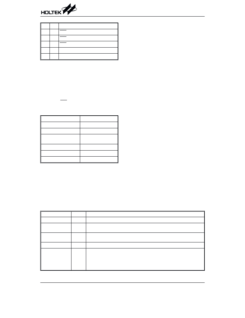
TO
PD
RESET Conditions
0
0
RES reset during power-up
u
u
RES reset during normal operation
0
1
RES wake-up HALT
1
u
WDT time-out during normal operation
1
1
WDT wake-up HALT
Note: u stands for unchanged
To guarantee that the system oscillator has started and
stabilized, the SST (System Start-up Timer) provides an
extra-delay of 1024 system clock pulses during system
power up or when the system awakes from a HALT
state.
When a system power-up occurs, the SST delay is
added during the reset period. But when the reset co-
mes from the RES pin, the SST delay is disabled. Any
wake-up from HALT will enable the SST delay.
The functional units chip reset status are shown below.
Program counter
000H
Interrupt
Disable
Prescaler
Clear
WDT
Clear. After master reset,
WDT begins counting
Timer/EventCounter(0/1) Off
Input/output ports
Input mode
SP
Points to the top of stack
Timer/Event Counter
Two timer/event counters are implemented in the
HT36A0. The Timer/Event Counter 0 and Timer/Event
Counter 1 contain 16-bit programmable count-up coun-
ters and the clock comes from the system clock divided
by 4.
There are three registers related to Timer/Event Coun-
ter 0; TMR0H (0CH), TMR0L (0DH), TMR0C (0EH).
Writing TMR0L only writes the data into a low byte
buffer, and writing TMR0H will write the data and the
contents of the low byte buffer into the Timer/Event
Counter 0 Preload register (16-bit) simultaneously. The
Timer/Event Counter 0 Preload register is changed by
writing TMR0H operations and writing TMR0L will keep
theTimer/EventCounter0Preloadregisterunchanged.
Reading TMR0H will also latch the TMR0L into the low
byte buffer to avoid a false timing problem. Reading
TMR0L returns the contents of the low byte buffer. In
other words, the low byte of the Timer/Event Counter 0
cannot be read directly. It must read the TMR0H first to
make the low byte contents of the Timer/Event Counter
0 latched into the buffer.
There are three registers related to the Timer/Event
Counter 1; TMR1H (0FH), TMR1L (10H), TMR1C (11H).
The Timer/Event Counter 1 operates in the same man-
ner as Timer/Event Counter 0.
The TMR0C is the Timer/Event Counter 0 control regis-
ter, which defines the Timer/Event Counter 0 options.
The Timer/Event Counter 1 has the same options with
Timer/Event Counter 0 and is defined by TMR1C.
TheTimer/eventCountercontrolregistersdefinetheop-
erating mode, counting enable or disable and active
edge.
The TM0, TM1 bits define the operating mode. The
Event count mode is used to count external events,
which means the clock source comes from an external
(TMR) pin. The Timer mode functions as a normal timer
with the clock source coming from the instruction clock.
The pulse width measurement mode can be used to
count the high or low level duration of the external signal
(TMR). The counting is based on the instruction clock.
In the Event count or Timer mode, once the timer/event
counter starts counting, it will count from the current
contents in the timer/event counter to FFFFH. Once
overflow occurs, the counter is reloaded from the
Timer/Event Counter Preload register and simulta-
neously generates the corresponding interrupt request
flag (T0F/T1F; bit 5/6 of INTC).
Label
Bits
Function
0~2
Unused bit, read as 0
TE
3
Define the TMR active edge of Timer/Event Counter 0
(0=active on low to high; 1=active on high to low)
TON
4
Enable/disable timer counting
(0=disable; 1=enable)
5
Unused bit, read as 0
TM0
TM1
6
7
Defines the operating mode
01=Event count mode (External clock)
10=Timer mode (Internal clock)
11=Pulse width measurement mode
00=Unused
TMR0C/TMR1C register
相關PDF資料 |
PDF描述 |
|---|---|
| HT3820(16DIP) | Sound Generator Circuit |
| HT3820(16SOP) | Sound Generator Circuit |
| HT3820A | Sound Generator Circuit |
| HT3820A(TO92A) | Analog IC |
| HT3820B | Sound Generator Circuit |
相關代理商/技術參數(shù) |
參數(shù)描述 |
|---|---|
| HT36A1 | 制造商:HOLTEK 制造商全稱:Holtek Semiconductor Inc 功能描述:Music Synthesizer 8-Bit MCU |
| HT36A2 | 制造商:HOLTEK 制造商全稱:Holtek Semiconductor Inc 功能描述:8-Bit Music Synthesizer MCU |
| HT36A3 | 制造商:HOLTEK 制造商全稱:Holtek Semiconductor Inc 功能描述:8-Bit Music Synthesizer MCU |
| HT36A4 | 制造商:HOLTEK 制造商全稱:Holtek Semiconductor Inc 功能描述:Music Synthesizer 8-Bit MCU |
| HT36A4_07 | 制造商:HOLTEK 制造商全稱:Holtek Semiconductor Inc 功能描述:Music Synthesizer 8-Bit MCU |
發(fā)布緊急采購,3分鐘左右您將得到回復。