- 您現(xiàn)在的位置:買賣IC網(wǎng) > PDF目錄370699 > HSMS-285A Surface Mount Microwave Schottky Detector Diodes in SOT-323(表貼型微波肖特基檢測二極管(SOT-323封裝)) PDF資料下載
參數(shù)資料
| 型號: | HSMS-285A |
| 英文描述: | Surface Mount Microwave Schottky Detector Diodes in SOT-323(表貼型微波肖特基檢測二極管(SOT-323封裝)) |
| 中文描述: | 表面安裝微波肖特基二極管探測器采用SOT - 323(表貼型微波肖特基檢測二極管(采用SOT - 323封裝)) |
| 文件頁數(shù): | 9/12頁 |
| 文件大小: | 117K |
| 代理商: | HSMS-285A |
9
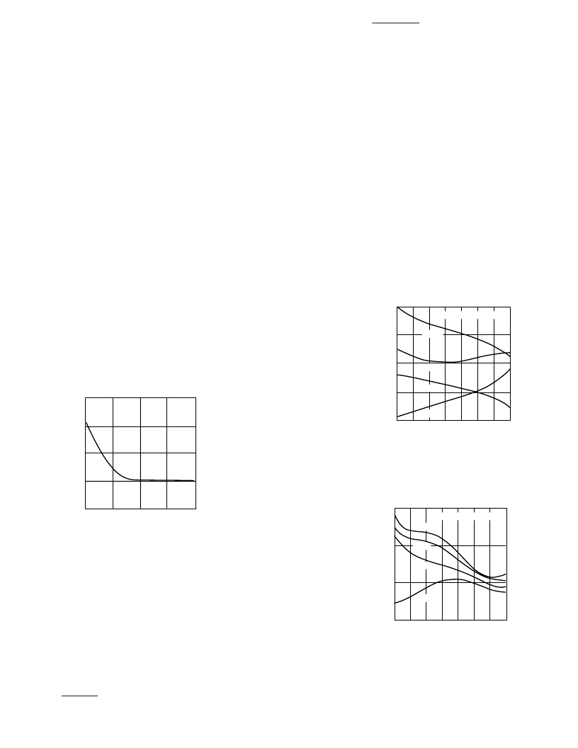
Flicker Noise
Reference to Figure 5 will show
that there is a junction of metal,
silicon, and passivation around the
rim of the Schottky contact. It is in
this three-way junction that flicker
noise
[7]
is generated. This noise
can severely reduce the sensitivity
of a crystal video receiver utilizing
a Schottky detector circuit if the
video frequency is below the noise
corner. Flicker noise can be
substantially reduced by the
elimination of passivation, but
such diodes cannot be mounted in
non-hermetic packages. p-type
silicon Schottky diodes have the
least flicker noise at a given value
of external bias (compared to n-
type silicon or GaAs). At zero bias,
such diodes can have extremely
low values of flicker noise. For the
HSMS-285A series, the noise
temperature ratio is given in
Figure 29.
N
FREQUENCY (Hz)
15
10
5
0
-5
10
100
1000
10000
100000
Figure 29. Typical Noise
Temperature Ratio.
Noise temperature ratio is the
quotient of the diode’s noise
power (expressed in dBV/Hz)
divided by the noise power of an
ideal resistor of resistance R = R
V
.
For an ideal resistor R, at 300
°
K,
the noise voltage can be computed
from
v = 1.287 X 10
-10
√
R volts/Hz
which can be expressed as
20 log
10
v
dBV/Hz
Thus, for a diode with R
V
= 9K
,
the noise voltage is 12.2 nV/Hz or
-158 dBV/Hz. On the graph of
Figure 26, -158 dBV/Hz would
replace the zero on the vertical
scale to convert the chart to one of
absolute noise voltage vs.
frequency.
Temperature Compensation
The compression of the detector’s
transfer curve is beyond the scope
of this data sheet, but some
general comments can be made.
As was given earlier, the diode’s
video resistance is given by
8.33 X 10
-5
nT
R
= ––––––––––––
I
S
+ I
b
where T is the diode’s tempera-
ture in
°
K.
As can be seen, temperature has a
strong effect upon R
V
, and this
will in turn affect video bandwidth
and input RF impedance. A glance
at Figure 7 suggests that the
proper choice of bias current in
the HSMS-286A series can mini-
mize variation over temperature.
The detector circuits described
earlier were tested over tempera-
ture. The 915 MHz voltage doubler
using the HSMS-286C series pair
produced the output voltages as
shown in Figure 30. The use of
3
μ
A of bias resulted in the highest
voltage sensitivity, but at the cost
of a wide variation over tempera-
ture. Dropping the bias to 1
μ
A
produced a detector with much
less temperature variation.
[7]
Hewlett-Packard Application Note 965-3,
Flicker Noise in Schottky Diodes.
A similar experiment was con-
ducted with the HSMS-286B in the
5.8 GHz detector. Once again,
reducing the bias to some level
under 3
μ
A stabilized the output of
the detector over a wide tempera-
ture range.
It should be noted that curves
such as those given in Figures 30
and 31 are highly dependent upon
the exact design of the input
impedance matching network.
The designer will have to experi-
ment with bias current using his
specific design.
Figure 30. Output Voltage vs.
Temperature and Bias Current in the
915 MHz Voltage Doubler using the
HSMS-286C.
-55
-35
-15
5
85
45
65
O
TEMPERATURE (
°
C)
25
40
80
60
120
100
INPUT POWER = –30 dBm
3.0
μ
A
1.0
μ
A
10
μ
A
0.5
μ
A
Figure 31. Output Voltage vs.
Temperature and Bias Current in the
5.80 GHz Voltage Detector using the
HSMS-286B Schottky.
O
TEMPERATURE (
°
C)
5
-55
15
35
25
INPUT POWER = –30 dBm
3.0
μ
A
10
μ
A
1.0
μ
A
0.5
μ
A
-35
-15
5
85
45
65
25
相關PDF資料 |
PDF描述 |
|---|---|
| HSMS-286A | Surface Mount Microwave Schottky Detector Diodes in SOT-323(表貼型微波肖特基檢測二極管(SOT-323封裝)) |
| HSMS-286K | Surface Mount RF Schottky Detector Diodes in SOT-363(表貼型射頻肖特基檢測二極管(SOT-363封裝)) |
| HSMS-286L | Surface Mount RF Schottky Detector Diodes in SOT-363(表貼型射頻肖特基檢測二極管(SOT-363封裝)) |
| HSMS-286P | Surface Mount RF Schottky Detector Diodes in SOT-363(表貼型射頻肖特基檢測二極管(SOT-363封裝)) |
| HSMS-286R | Surface Mount RF Schottky Detector Diodes in SOT-363(表貼型射頻肖特基檢測二極管(SOT-363封裝)) |
相關代理商/技術參數(shù) |
參數(shù)描述 |
|---|---|
| HSMS-285ASERIES | 制造商:未知廠家 制造商全稱:未知廠家 功能描述:Surface Mount Microwave Schottky Detector Diodes in SOT-323 (SC-70) (155K in pdf) |
| HSMS-285B | 制造商:HP 制造商全稱:Agilent(Hewlett-Packard) 功能描述:Surface Mount Zero Bias Schottky Detector Diodes |
| HSMS-285B-BLK | 制造商:HP 制造商全稱:Agilent(Hewlett-Packard) 功能描述:Surface Mount Zero Bias Schottky Detector Diodes |
| HSMS-285B-BLKG | 功能描述:射頻檢測器 RF/ID below 1.5GHz RoHS:否 制造商:Skyworks Solutions, Inc. 配置: 頻率范圍:650 MHz to 3 GHz 最大二極管電容: 最大工作溫度:+ 85 C 最小工作溫度:- 40 C 封裝 / 箱體:SC-88 封裝:Reel |
| HSMS-285B-G | 制造商:Avago Technologies 功能描述:HSMS-285B zero-bias Schottky detector |
發(fā)布緊急采購,3分鐘左右您將得到回復。