- 您現(xiàn)在的位置:買賣IC網(wǎng) > PDF目錄371871 > HN4G01J (Toshiba Corporation) Audio Frequency General Purpose Amplifier Applications PDF資料下載
參數(shù)資料
| 型號: | HN4G01J |
| 廠商: | Toshiba Corporation |
| 英文描述: | Audio Frequency General Purpose Amplifier Applications |
| 中文描述: | 通用音頻放大器應(yīng)用 |
| 文件頁數(shù): | 1/6頁 |
| 文件大小: | 495K |
| 代理商: | HN4G01J |
HN4G01J
2007-11-01
1
TOSHIBA Multi Chip Discrece Device
HN4G01J
Audio Frequency General Purpose Amplifier Applications
Q1
z
Small package (Dual type)
z
High voltage and high current
: V
CEO
= 50V, I
C
= 150mA (max)
z
High h
FE
: h
FE
= 120~400
z
Excellent h
FE
linearity
: h
FE
(I
C
= 0.1mA) / h
FE
(I
C
= 2mA) = 0.95 (typ.)
Q2
z
Incorporating a bias resistor into a transistor reduces parts count.
Reducing the parts count enable the manufacture of ever more
compact equipment and save assembly cost.
Q1 : 2SC4837F
Q2 : RN1103F
Q1 Absolute Maximum Ratings
(Ta = 25°C)
Characteristic
Symbol
Rating
Unit
Collector-base voltage
V
CBO
60
V
Collector-emitter voltage
V
CEO
50
V
Emitter-base voltage
V
EBO
5
V
Collector current
I
C
150
mA
Base current
Q2 Absolute Maximum Ratings
(Ta = 25°C)
I
B
30
mA
Characteristic
Symbol
Rating
Unit
Collector-base voltage
V
CBO
50
V
Collector-emitter voltage
V
CEO
50
V
Emitter-base voltage
V
EBO
10
V
Collector current
Absolute Maximum Ratings
(Ta = 25°C) (Q1,Q2Common)
I
C
100
mA
Characteristic
Symbol
Rating
Unit
Collector power dissipation
P
C
*
300
mW
Junction temperature
T
j
150
°
C
Storage temperature range
T
stg
55~150
°
C
Note: Using continuously under heavy loads (e.g. the application of high temperature/current/voltage and the
significant change in temperature, etc.) may cause this product to decrease in the reliability significantly even
if the operating conditions (i.e. operating temperature/current/voltage, etc.) are within the absolute maximum
ratings.
Please design the appropriate reliability upon reviewing the Toshiba Semiconductor Reliability Handbook
(“Handling Precautions”/“Derating Concept and Methods”) and individual reliability data (i.e. reliability test
report and estimated failure rate, etc).
* Total rating.
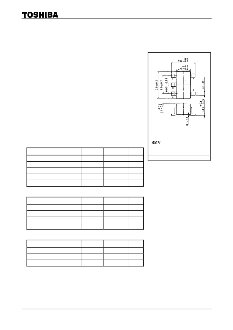
1.BASE1
2.EMITTER
3.BASE2
4.COLLECTOR2
5.COLLECTOR1
(B1)
(E)
(B2)
(C2)
(C1)
JEDEC
JEITA
TOSHIBA
Weight: 0.014g(Typ.)
―
―
2-3L1A
Unit: mm
相關(guān)PDF資料 |
PDF描述 |
|---|---|
| HN4K03JU | N CHANNEL MOS TYPE (HIGH SPEED SWITCHING, ANALOG SWITCH APPLICATIONS) |
| HN549 | NPN Silicon Epitaxial Planar Transistor |
| HN5550 | NPN Silicon Expitaxial Planar Transistor for general purpose, high voltage amplifier applications |
| HN5551 | NPN Silicon Expitaxial Planar Transistor for general purpose, high voltage amplifier applications |
| HN556 | PNP Silicon Epitaxial Planar Transistor for switching and AF applications |
相關(guān)代理商/技術(shù)參數(shù) |
參數(shù)描述 |
|---|---|
| HN4G-41-1 | 制造商:HARTWELL (SOUTHCO) 功能描述: |
| HN4G-41-2 | 制造商:HARTWELL (SOUTHCO) 功能描述: |
| HN4G-42-1 | 制造商:HARTWELL (SOUTHCO) 功能描述: |
| HN4G432 | 制造商:n/a 功能描述:Ships in 2 days |
| HN4G-43-2 | 制造商:HARTWELL (SOUTHCO) 功能描述: |
發(fā)布緊急采購,3分鐘左右您將得到回復(fù)。