- 您現(xiàn)在的位置:買賣IC網(wǎng) > PDF目錄370642 > HMMC-3104 DC-16 GHz Packaged Divide-by-4 Prescaler(DC-16 GHz 封裝的砷化鎵HBT單片微波集成電路除4定標器) PDF資料下載
參數(shù)資料
| 型號: | HMMC-3104 |
| 英文描述: | DC-16 GHz Packaged Divide-by-4 Prescaler(DC-16 GHz 封裝的砷化鎵HBT單片微波集成電路除4定標器) |
| 中文描述: | 的DC - 16 GHz的包裝分頻4分頻器(直流- 16千兆赫封裝的砷化鎵HBT的單片微波集成電路除四定標器) |
| 文件頁數(shù): | 2/6頁 |
| 文件大小: | 64K |
| 代理商: | HMMC-3104 |
2
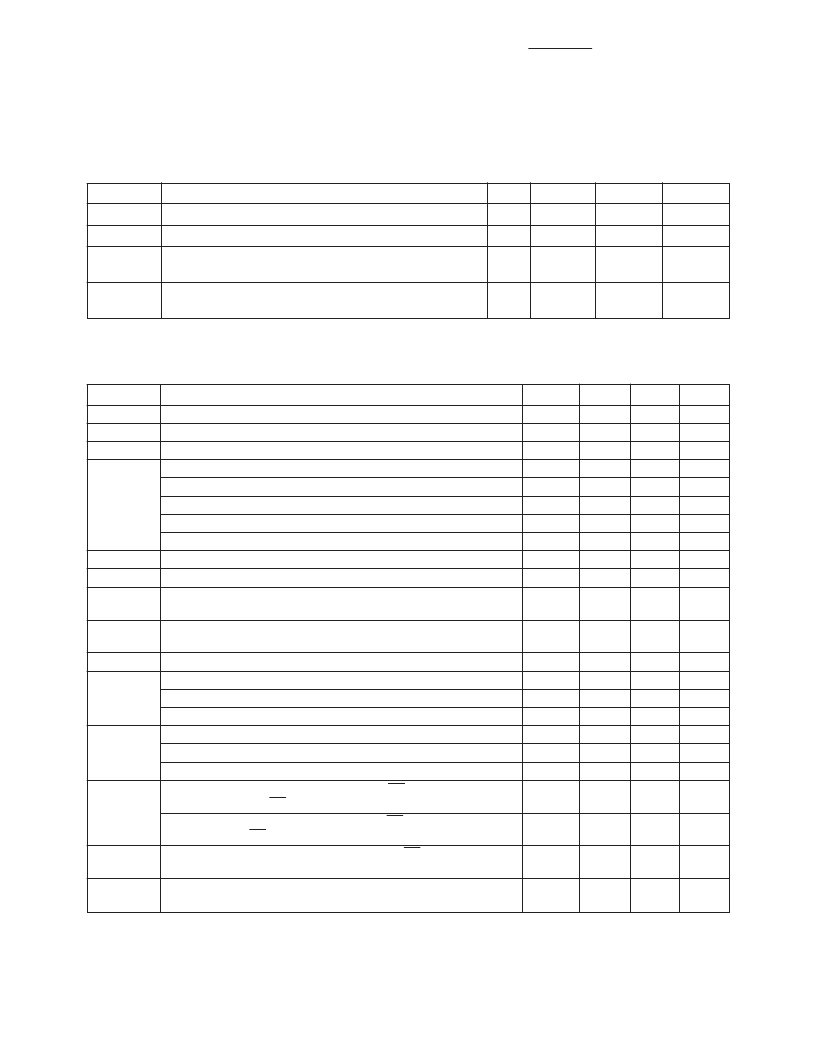
HMMC-3104 DC Specifications/Physical Properties,
(T
A
= 25
°
C, V
CC
- V
EE
= 5.0 V unless otherwise listed)
Symbol
Parameters and Test Conditions
Units
Min.
Typ.
Max.
V
CC
- V
EE
|
CC
|or |
EE
| Bias Supply Current
V
RFin(q)
Quiescent DC Voltage appearing at all RF Ports
V
RFout(q)
Operating Bias Supply Difference
[1]
volts
mA
4.5
68
5.0
80
6.5
92
volts
V
CC
V
Logic
Nominal ECL Logic Level
(V
Logic
contact self-bias voltage, generated on-chip)
volts
V
CC
- 1.45 V
CC
- 1.35 V
CC
- 1.25
Note:
1. Prescaler will operate over full specified supply voltage range. V
CC
or V
EE
not to exceed limits specified in Absolute Maximum Ratings section.
RF Specifications,
(T
A
= 25
°
C, Z
O
= 50
, V
CC
- V
EE
= 5.0 V)
Symbol
Parameters and Test Conditions
in(max)
Maximum input frequency of operation
in(min)
Minimum input frequency of operation
[1]
(P
in
= -10 dBm)
Self-Osc.
Output Self-Oscillation Frequency
[2]
@ DC, (Square-wave input)
@
in
= 500 MHz, (Sine-wave input)
P
in
in
= 1 to 10 GHz
in
= 10 to 12 GHz
in
= 12 to 15 GHz
RL
Small-Signal Input/Output Return Loss (@
in
< 12 GHz)
S
12
Small-Signal Reverse Isolation (@
in
< 12 GHz)
N
SSB Phase Noise (@ P
in
= 0 dBm, 100 kHz offset
from a
out
= 1.2 GHz Carrier
Jitter
Input Signal Time Variation @ Zero-Crossing
(
in
= 10 GHz, P
in
= -10 dBm)
T
r
or T
f
Output Transition Time (10% to 90% rise/fall time)
@
out
< 1 GHz
P
out[3]
out
= 2.5 GHz
out
= 3.5 GHz
@
out
< 1 GHz
|V
out(p-p)
|
[4]
out
= 2.5 GHz
out
= 3.5 GHz
out
power level appearing at RF
in
or RF
in
(@
in
= 12 GHz,
Unused RF
out
or RF
out
unterminated
)
out
power level appearing at RF
in
or RF
in
(@
in
= 12 GHz,
Both RF
out
& RF
out
terminated
)
P
feedthru
Power level of
in
appearing at RF
out
or RF
out
(@
in
= 12 GHz, P
in
= 0 dBm, Referred to P
in
(
in
))
H
2
Second harmonic distortion output level
(@
out
= 3.0 GHz, Referred to P
out
(
out
))
Notes:
1. For sine-wave input signal. Prescaler will operate down to D.C. for square-wave input signal. Minimum divide frequency limited by
input slew-rate.
2. Prescaler can exhibit this output signal under bias in the absence of an RF input signal. This condition may be eliminated by use of the
input DC offset technique described on page 3.
3. Fundamental of output square wave’s Fourier Series.
4. Square wave amplitude calculated from P
out
.
Units
GHz
GHz
GHz
dBm
dBm
dBm
dBm
dBm
dB
dB
dBc/Hz
Min.
16
Typ.
18
0.2
3.4
>-25
>-20
>-25
>-15
>-10
15
30
-153
Max.
0.5
-15
-15
-15
-10
-4
+10
+10
+10
+10
+4
ps
1
ps
70
6
5.5
2.0
0.99
0.94
0.63
-40
dBm
dBm
dBm
volts
volts
volts
dBm
4
3.5
0
P
Spitback
dBm
-47
dBc
-23
dBc
-25
相關PDF資料 |
PDF描述 |
|---|---|
| HMMC-3108 | DC-16 GHz Packaged Divide-by-8 Prescaler(DC-16 GHz 封裝的砷化鎵HBT單片微波集成電路除8定標器) |
| HMMC-3124 | DC-12 GHz Packaged High Efficiency Divide-by-4 Prescaler(DC-12 GHz 封裝的高效除4定標器) |
| HMMC-3128 | DC-12 GHz Packaged High Efficiency Divide-by-8 Prescaler(DC-12 GHz 封裝的高效除8定標器) |
| HMMC-5003 | 4 GHz Wideband Preamplifier/Amplifier(4 GHz 寬帶前級放大器/放大器) |
| HMMC-5004 | 3 GHz Wideband Power Amplifier(3 GHz寬帶功率放大器) |
相關代理商/技術參數(shù) |
參數(shù)描述 |
|---|---|
| HMMC-3104-BLK | 制造商:Agilent Technologies 功能描述:PRESCALER 5V 1/4 16000MHZ 8SOIC - Bulk |
| HMMC-3104-TR1 | 制造商:Agilent Technologies 功能描述:PRESCALER 5V 1/4 16000MHZ 8SOIC,MAX REEL SIZE=500 - Tape and Reel |
| HMMC-3108 | 制造商:未知廠家 制造商全稱:未知廠家 功能描述:SO-8 SMT 0.5-16 GHz GaAs HBT prescalers |
| HMMC-3108-BLK | 制造商:Agilent Technologies 功能描述:PRESCALER 5V 1/8 16000MHZ 8SOIC - Bulk |
| HMMC-3108-TR1 | 制造商:Agilent Technologies 功能描述:PRESCALER 5V 1/8 16000MHZ 8SOIC, MAX REEL ZIE=500 - Tape and Reel |
發(fā)布緊急采購,3分鐘左右您將得到回復。