- 您現(xiàn)在的位置:買賣IC網(wǎng) > PDF目錄299176 > HK10051N2S (TAIYO YUDEN CO LTD) 1 ELEMENT, 0.0012 uH, FERRITE-CORE, GENERAL PURPOSE INDUCTOR, SMD PDF資料下載
參數(shù)資料
| 型號: | HK10051N2S |
| 廠商: | TAIYO YUDEN CO LTD |
| 元件分類: | 通用定值電感 |
| 英文描述: | 1 ELEMENT, 0.0012 uH, FERRITE-CORE, GENERAL PURPOSE INDUCTOR, SMD |
| 封裝: | CHIP, 0402, ROHS COMPLIANT |
| 文件頁數(shù): | 10/21頁 |
| 文件大小: | 755K |
| 代理商: | HK10051N2S |
mlci0109_reli-PRP13
mlci0109_reli_e-01
■ PRECAUTIONS
*This catalog contains the typical specication only due to the limitation of space. When you consider the purchase of our products, please check our specication.
For details of each product (characteristics graph, reliability information, precautions for use, and so on), see our Web site (http://www.ty-top.com/) or CD catalogs.
Precautions on the use of Multilayer chip Inductors, Multilayer chip inductors for high frequency, Multilayer ferrite chip beads
1. Circuit Design
Precautions
◆Verication of operating environment, electrical rating and performance
1. A malfunction in medical equipment, spacecraft, nuclear reactors, etc. may cause serious harm to human life or have severe social ramications.
As such, any inductors to be used in such equipment may require higher safety and/or reliability considerations and should be clearly differentiated from
components used in general purpose applications.
◆Operating Current(Verication of Rated current)
1. The operating current for inductors must always be lower than their rated values.
2. Do not apply current in excess of the rated value because the inductance may be reduced due to the magnetic saturation effect.
2. PCB Design
Precautions
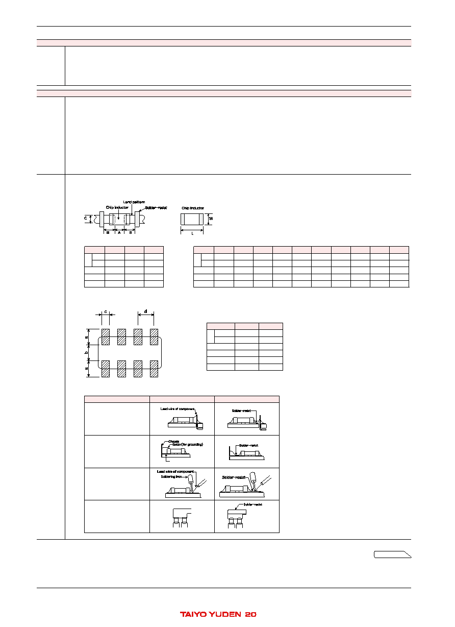
◆Pattern congurations(Design of Land-patterns)
1. When inductors are mounted on a PCB, the size of land patterns and the amount of solder used(size of llet)can directly affect inductor performance.
Therefore, the following items must be carefully considered in the design of solder land patterns:
(1)The amount of solder applied can affect the ability of chips to withstand mechanical stresses which may lead to breaking or cracking. Therefore, when
designing land-patterns it is necessary to consider the appropriate size and conguration of the solder pads which in turn determines the amount of
solder necessary to form the llets.
(2)When more than one part is jointly soldered onto the same land or pad, the pad must be designed so that each component's soldering point is separated
by solder-resist.
(3)The larger size of land patterns and amount of solder, the smaller Q value after mounting on PCB. It makes higher the Q value to design land patterns
smaller than terminal electrode of chips.
◆Pattern congurations(Inductor layout on panelized[breakaway]PC boards)
1. After inductors have been mounted on the boards, chips can be subjected to mechanical stresses in subsequent manufacturing processes(PCB cutting,
board inspection, mounting of additional parts, assembly into the chassis, wave soldering the reow soldered boards etc.)For this reason, planning pattern
congurations and the position of SMD inductors should be carefully performed to minimize stress.
Technical
consider-
ations
◆Pattern congurations(Design of Land-patterns)
1. The following diagrams and tables show some examples of recommended patterns to prevent excessive solder amounts(larger llets which extend above
the component end terminations).Examples of improper pattern designs are also shown.
(1)Recommended land dimensions for a typical chip inductor land patterns for PCBs
Recommended land dimensions for wave-soldering
Recommended land dimensions for reow-soldering
Type
1608
2125
3216
Size
L
1.6
2.0
3.2
W
0.8
1.25
1.6
A
0.8~1.0 1.0~1.4 1.8~2.5
B
0.5~0.8 0.8~1.5 0.8~1.7
C
0.6~0.8 0.9~1.2 1.2~1.6
(Unit:mm)
Type
0402
0603
1005
105
1608
2012
2125
2016
3216
2520
Size
L
0.4
0.6
1.0
1.6
2.0
3.2
2.5
W
0.2
0.3
0.5
0.6
0.8
1.25
1.6
2.0
A
0.15~0.25 0.20~0.30 0.45~0.55 0.50~0.55 0.8~1.0 0.8~1.2 0.8~1.2 0.8~1.2 1.8~2.5 1.0~1.4
B
0.10~0.20 0.20~0.30 0.40~0.50 0.30~0.40 0.6~0.8 0.8~1.2 0.8~1.2 0.8~1.2 0.6~1.5 0.6~1.0
C
0.15~0.30 0.25~0.40 0.45~0.55 0.60~0.70 0.6~0.8 0.9~1.6 0.9~1.6 1.2~2.0 1.2~2.0 1.8~2.2
(Unit:mm)
Excess solder can affect the ability of chips to withstand mechanical stresses. Therefore, please take proper precautions when designing land-patterns.
Recommended land dimension for Reow-soldering
Type
3216
2010
Size
L
3.2
2.0
W
1.6
1.0
a
0.7~0.9
0.5~0.6
b
0.8~1.0
0.5~0.6
c
0.4~0.5
0.2~0.3
d
0.8
0.5
(Unit:mm)
(2)Examples of good and bad solder application
Item
Not recommended
Recommended
Mixed mounting of SMD
and leaded components
Component placement
close to the chassis
Hand-soldering of leaded
components near mounted
components
Horizontal component
placement
To next page
相關PDF資料 |
PDF描述 |
|---|---|
| HK1005R10K | 1 ELEMENT, 0.1 uH, FERRITE-CORE, GENERAL PURPOSE INDUCTOR, SMD |
| HK100582NK | 1 ELEMENT, 0.082 uH, FERRITE-CORE, GENERAL PURPOSE INDUCTOR, SMD |
| HK100568NK | 1 ELEMENT, 0.068 uH, FERRITE-CORE, GENERAL PURPOSE INDUCTOR, SMD |
| HK10058N2K | 1 ELEMENT, 0.0082 uH, FERRITE-CORE, GENERAL PURPOSE INDUCTOR, SMD |
| HK10055N6K | 1 ELEMENT, 0.0056 uH, FERRITE-CORE, GENERAL PURPOSE INDUCTOR, SMD |
相關代理商/技術參數(shù) |
參數(shù)描述 |
|---|---|
| HK10051N2S-T | 功能描述:固定電感器 INDCTR HIFREQ MLTLYR 0402 1.20.3nH RoHS:否 制造商:AVX 電感:10 uH 容差:20 % 最大直流電流:1 A 最大直流電阻:0.075 Ohms 工作溫度范圍:- 40 C to + 85 C 自諧振頻率:38 MHz Q 最小值:40 尺寸:4.45 mm W x 6.6 mm L x 2.92 mm H 屏蔽:Shielded 端接類型:SMD/SMT 封裝 / 箱體:6.6 mm x 4.45 mm |
| HK10051N2S-T | 制造商:TAIYO YUDEN 功能描述:Inductor Series:LG HK 制造商:TAIYO YUDEN 功能描述:INDUCTOR |
| HK-1005-1N2STK | 功能描述:固定電感器 1.2nH 300mA 0.3nH RoHS:否 制造商:AVX 電感:10 uH 容差:20 % 最大直流電流:1 A 最大直流電阻:0.075 Ohms 工作溫度范圍:- 40 C to + 85 C 自諧振頻率:38 MHz Q 最小值:40 尺寸:4.45 mm W x 6.6 mm L x 2.92 mm H 屏蔽:Shielded 端接類型:SMD/SMT 封裝 / 箱體:6.6 mm x 4.45 mm |
| HK10051N5S-T | 功能描述:固定電感器 INDCTR HIFREQ MLTLYR 0402 1.50.3nH RoHS:否 制造商:AVX 電感:10 uH 容差:20 % 最大直流電流:1 A 最大直流電阻:0.075 Ohms 工作溫度范圍:- 40 C to + 85 C 自諧振頻率:38 MHz Q 最小值:40 尺寸:4.45 mm W x 6.6 mm L x 2.92 mm H 屏蔽:Shielded 端接類型:SMD/SMT 封裝 / 箱體:6.6 mm x 4.45 mm |
| HK-1005-1N5STK | 功能描述:固定電感器 1.5nH 300mA 0.3nH RoHS:否 制造商:AVX 電感:10 uH 容差:20 % 最大直流電流:1 A 最大直流電阻:0.075 Ohms 工作溫度范圍:- 40 C to + 85 C 自諧振頻率:38 MHz Q 最小值:40 尺寸:4.45 mm W x 6.6 mm L x 2.92 mm H 屏蔽:Shielded 端接類型:SMD/SMT 封裝 / 箱體:6.6 mm x 4.45 mm |
發(fā)布緊急采購,3分鐘左右您將得到回復。