- 您現(xiàn)在的位置:買賣IC網(wǎng) > PDF目錄299176 > HIP0050IB (INTERSIL CORP) 0.3 A BUF OR INV BASED PRPHL DRVR, PDSO24 PDF資料下載
參數(shù)資料
| 型號(hào): | HIP0050IB |
| 廠商: | INTERSIL CORP |
| 元件分類: | Peripheral Driver |
| 英文描述: | 0.3 A BUF OR INV BASED PRPHL DRVR, PDSO24 |
| 封裝: | PLASTIC, MS-013-AD, SOIC-24 |
| 文件頁數(shù): | 5/7頁 |
| 文件大小: | 156K |
| 代理商: | HIP0050IB |
5
HIP0050
Pin Descriptions
VCC Power Pin
The VCC pin is the positive 5V logic voltage supply input for
the IC. The normal operating voltage range is 4.5V to 5.5V.
When switched on, the POR forces all outputs off.
SCK Serial Clock Pin
SCK is the clock input for the SPI Interface. Output ON/OFF
control data is clocked into an eight stage shift register on
the rising edge of an external clock. This input has a Schmitt
trigger.
SI Serial Data In Pin
SI is the Serial Data Input Pin for the SPI Interface. The eight
power outputs are controlled by the serial data via the output
data buffer. This input has a Schmitt Trigger.
STR Strobe Pin for the SPI Interface
When the STR Pin is high, data from the 8-bit shift register is
passed into the output data buffers where it controls the ON-
OFF state of each output driver. The data is latched in the
output data buffers when STR goes low. This input has a
Schmitt trigger.
SO Serial Data Out Pin
The serial data out allows other ICs to be serially cascaded.
For example, a 10-bit LED driver may be located behind the
HIP0050. A controlling microprocessor may then clock out
18-bits of information and simultaneously strobe both parts.
The cascaded ICs may be the same or different from the
HIP0050.
DR0 - DR7 Outputs 0 Thru 7
The drain output pins of the DMOS Power Drivers are capa-
ble of sinking 300mA. Each output has short circuit protection to
independently shutdown the output under excessive high load
current conditions.
FLT Fault Flag
The fault flag pin indicates an over-current in any one of the
output drivers. (It is not an indicator for the thermal shutdown
mode.) The FLT output is active low and can sink 1.6mA
when activated. When latched low, it will remain latched until
the next data strobe.
EN Enable Pin
The enable pin is an active low enable function for all eight
output drivers. When EN is high, drive from the output data
buffer is held low and all output drivers are disabled. When
EN is low, the output drivers are enabled and data in the 8-bit
shift register is transparent to the output data buffer. This input
has a Schmitt trigger.
LGND and GND Pins
The LGND Pin is the 5V Logic Supply Ground for the IC and
GND is a common ground for the power output drivers.
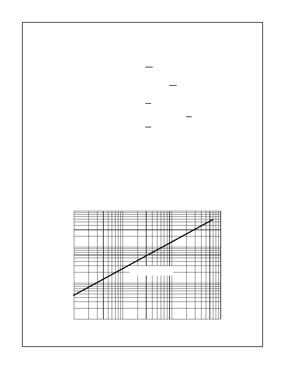
FIGURE 2. MAXIMUM SINGLE PULSE ENERGY SAFE OPERATING AREA FOR EACH CLAMPED OUTPUT DRIVER, TA = 25
oC
0.1
1
10
100
1
10
100
TIME (ms)
EN
E
R
G
Y
(
m
J
)
SAFE OPERATING AREA
BELOW LINE
1000
相關(guān)PDF資料 |
PDF描述 |
|---|---|
| HIP1030AS | 1.6 A BUF OR INV BASED PRPHL DRVR, PSFM5 |
| HK10051N2S | 1 ELEMENT, 0.0012 uH, FERRITE-CORE, GENERAL PURPOSE INDUCTOR, SMD |
| HK1005R10K | 1 ELEMENT, 0.1 uH, FERRITE-CORE, GENERAL PURPOSE INDUCTOR, SMD |
| HK100582NK | 1 ELEMENT, 0.082 uH, FERRITE-CORE, GENERAL PURPOSE INDUCTOR, SMD |
| HK100568NK | 1 ELEMENT, 0.068 uH, FERRITE-CORE, GENERAL PURPOSE INDUCTOR, SMD |
相關(guān)代理商/技術(shù)參數(shù) |
參數(shù)描述 |
|---|---|
| HIP0050IB96 | 制造商:Rochester Electronics LLC 功能描述:- Bulk |
| HIP0050IB96S2300 | 制造商:Rochester Electronics LLC 功能描述:- Bulk |
| HIP0050IP | 制造商:Rochester Electronics LLC 功能描述:- Bulk |
| HIP0051 | 制造商:INTERSIL 制造商全稱:Intersil Corporation 功能描述:0.25A/50V Octal Low Side Power Driver with Serial Bus Control |
| HIP0051IB | 制造商:INTERSIL 制造商全稱:Intersil Corporation 功能描述:0.25A/50V Octal Low Side Power Driver with Serial Bus Control |
發(fā)布緊急采購,3分鐘左右您將得到回復(fù)。