- 您現在的位置:買賣IC網 > PDF目錄299176 > HIN235CP (INTERSIL CORP) LINE TRANSCEIVER, PDIP24 PDF資料下載
參數資料
| 型號: | HIN235CP |
| 廠商: | INTERSIL CORP |
| 元件分類: | Line Driver or Receiver |
| 英文描述: | LINE TRANSCEIVER, PDIP24 |
| 封裝: | PLASTIC, DIP-24 |
| 文件頁數: | 6/13頁 |
| 文件大?。?/td> | 290K |
| 代理商: | HIN235CP |
504
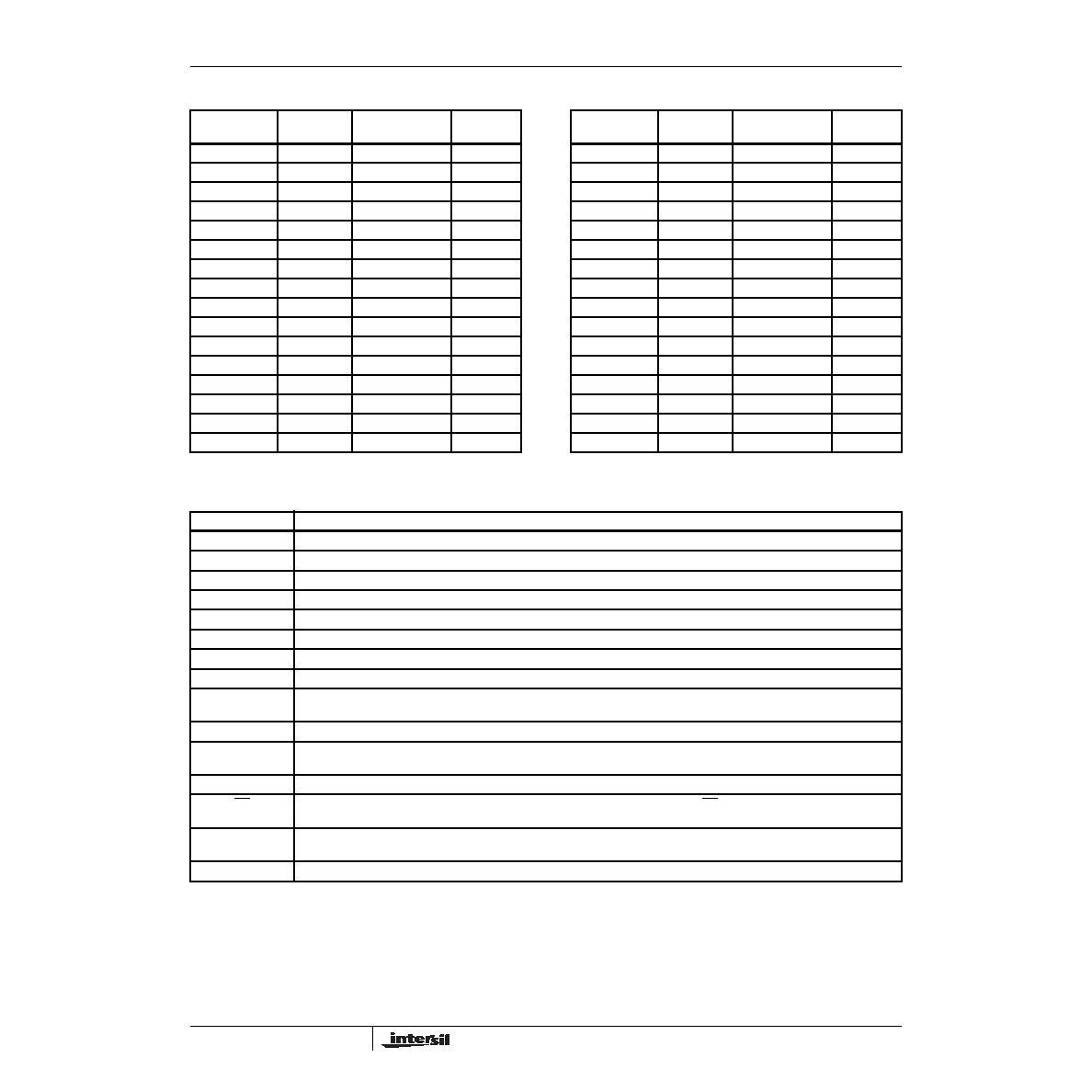
Ordering Information
Pin Descriptions
PART
NUMBER
TEMP.
RANGE (oC)
PACKAGE
PKG. NO.
HIN230CB
0 to 70
20 Ld SOIC
M20.3
HIN230IB
-40 to 85
20 Ld SOIC
M20.3
HIN231CB
0 to 70
16 Ld SOIC
M16.3
HIN231IB
-40 to 85
16 Ld SOIC
M16.3
HIN232CP
0 to 70
16 Ld PDIP
E16.3
HIN232CB
0 to 70
16 Ld SOIC
M16.3
HIN232IP
-40 to 85
16 Ld PDIP
E16.3
HIN232IB
-40 to 85
16 Ld SOIC
M16.3
HIN233CP
0 to 70
20 Ld PDIP
E20.3
HIN234CB
0 to 70
16 Ld SOIC
M16.3
HIN234IB
-40 to 85
16 Ld SOIC
M16.3
HIN235CP
0 to 70
24 Ld PDIP
E24.3
HIN236CP
0 to 70
24 Ld PDIP
E24.3
HIN236CB
0 to 70
24 Ld SOIC
M24.3
HIN236IP
-40 to 85
24 Ld PDIP
E24.3
HIN236IB
-40 to 85
24 Ld SOIC
M24.3
HIN237CP
0 to 70
24 Ld PDIP
E24.3
HIN237CB
0 to 70
24 Ld SOIC
M24.3
HIN237IP
-40 to 85
24 Ld PDIP
E24.3
HIN237IB
-40 to 85
24 Ld SOIC
M24.3
HIN238CP
0 to 70
24 Ld PDIP
E24.3
HIN238CB
0 to 70
24 Ld SOIC
M24.3
HIN238IP
-40 to 85
24 Ld PDIP
E24.3
HIN238IB
-40 to 85
24 Ld SOIC
M24.3
HIN239CB
0 to 70
24 Ld SOIC
M24.3
HIN239IB
-40 to 85
24 Ld SOIC
M24.3
HIN240CN
0 to 70
44 Ld MQFP
Q44.10X10
HIN240IN
-40 to 85
44 Ld MQFP
Q44.10X10
HIN241CB
0 to 70
28 Ld SOIC
M28.3
HIN241IB
-40 to 85
28 Ld SOIC
M28.3
HIN241CA
0 to 70
28 Ld SSOP
M28.209
HIN241IA
-40 to 85
28 Ld SSOP
M28.209
PART
NUMBER
TEMP.
RANGE (oC)
PACKAGE
PKG. NO.
PIN
FUNCTION
VCC
Power Supply Input 5V
±10%. HIN233 and HIN235 5V ±5%.
V+
Internally generated positive supply (+10V nominal), HIN231 and HIN239 requires +7.5V to +13.2V.
V-
Internally generated negative supply (-10V nominal).
GND
Ground lead. Connect to 0V.
C1+
External capacitor (+ terminal) is connected to this lead.
C1-
External capacitor (- terminal) is connected to this lead.
C2+
External capacitor (+ terminal) is connected to this lead.
C2-
External capacitor (- terminal) is connected to this lead.
TIN
Transmitter Inputs. These leads accept TTL/CMOS levels. An internal 400k
pull-up resistor to V
CC is
connected to each lead.
TOUT
Transmitter Outputs. These are RS-232 levels (nominally
±10V).
RIN
Receiver Inputs. These inputs accept RS-232 input levels. An internal 5k
pull-down resistor to GND is connected to each
input.
ROUT
Receiver Outputs. These are TTL/CMOS levels.
EN
Enable input. This is an active low input which enables the receiver outputs. With EN = 5V, the outputs are placed in a
high impedance state.
SD
Shutdown Input. With SD = 5V, the charge pump is disabled, the receiver outputs are in a high impedance state and the
transmitters are shut off.
NC
No Connect. No connections are made to these leads.
HIN230 thru HIN241
相關PDF資料 |
PDF描述 |
|---|---|
| HIN236IP | LINE TRANSCEIVER, PDIP24 |
| HIN237IP | LINE TRANSCEIVER, PDIP24 |
| HIN237IB | LINE TRANSCEIVER, PDSO24 |
| HIN237CP | LINE TRANSCEIVER, PDIP24 |
| HIN238IP | LINE TRANSCEIVER, PDIP24 |
相關代理商/技術參數 |
參數描述 |
|---|---|
| HIN235E | 制造商:INTERSIL 制造商全稱:Intersil Corporation 功能描述:+/-15kV, ESD-Protected, +5V Powered,RS-232 Transmitters/Receivers |
| HIN235ECP | 制造商:Rochester Electronics LLC 功能描述:- Bulk |
| HIN236 | 制造商:INTERSIL 制造商全稱:Intersil Corporation 功能描述:+5V Powered RS-232 Transmitters/Receivers |
| HIN236A | 制造商:INTERSIL 制造商全稱:Intersil Corporation 功能描述:High Speed +5V Powered RS-232 Transmitters/Receivers |
| HIN236ACA | 制造商:INTERSIL 制造商全稱:Intersil Corporation 功能描述:High Speed +5V Powered RS-232 Transmitters/Receivers |
發(fā)布緊急采購,3分鐘左右您將得到回復。