- 您現(xiàn)在的位置:買賣IC網(wǎng) > PDF目錄370584 > HIN209CP (Harris Corporation) 5V High-Speed RS-232 Transceivers with 0.1uF Capacitors PDF資料下載
參數(shù)資料
| 型號: | HIN209CP |
| 廠商: | Harris Corporation |
| 元件分類: | RS-232 |
| 英文描述: | 5V High-Speed RS-232 Transceivers with 0.1uF Capacitors |
| 中文描述: | 5V的高速RS - 232收發(fā)器與0.1uF電容 |
| 文件頁數(shù): | 2/14頁 |
| 文件大小: | 169K |
| 代理商: | HIN209CP |
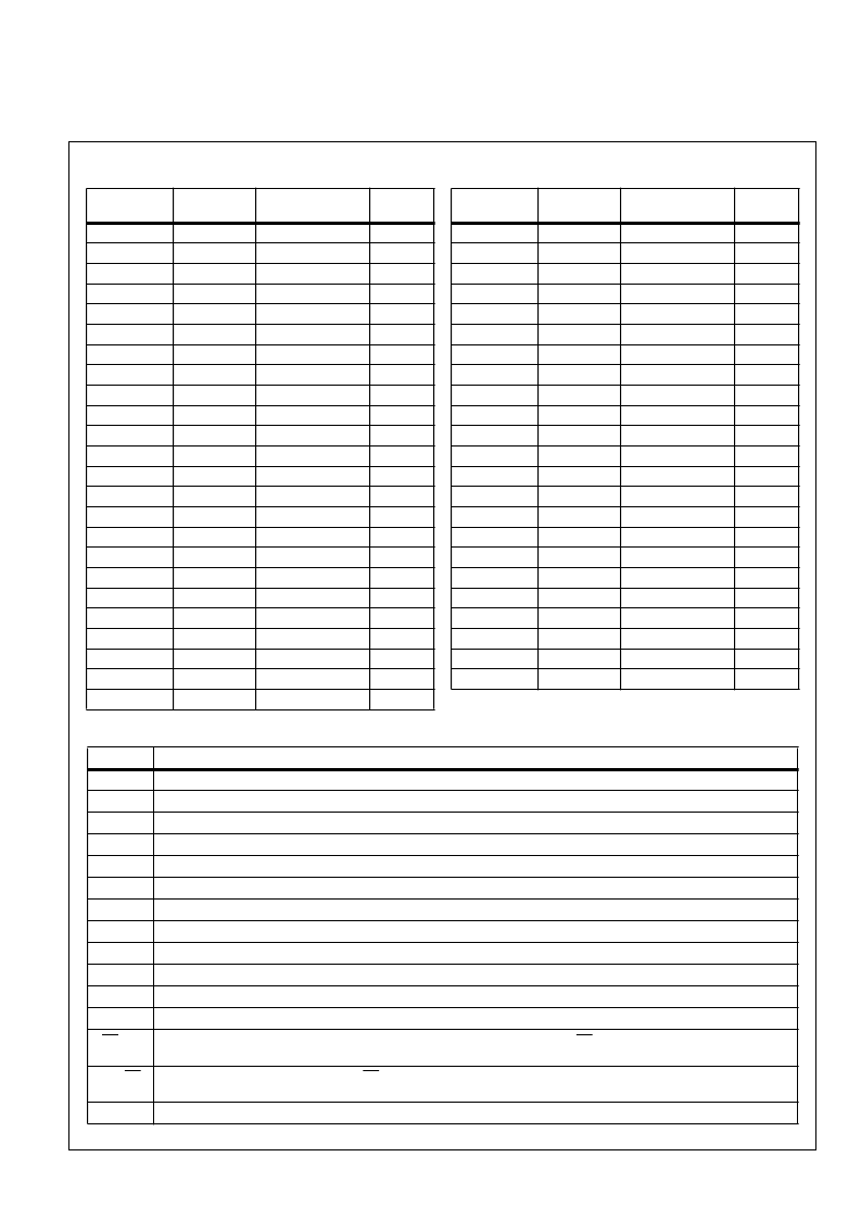
8-4
Ordering Information
PART NO.
TEMP.
RANGE (
o
C)
PACKAGE
PKG. NO.
HIN200CB
0 to 70
20 Ld SOIC
M20.3
HIN200IB
-40 to 85
20 Ld SOIC
M20.3
HIN201CB
0 to 70
16 Ld SOIC (W)
M16.3
HIN201IB
-40 to 85
16 Ld SOIC (W)
M16.3
HIN202CP
0 to 70
16 Ld PDIP
E16.3
HIN202CB
0 to 70
16 Ld SOIC (W)
M16.3
HIN202IP
-40 to 85
16 Ld PDIP
E16.3
HIN202CA
0 to 70
16 Ld SSOP
M16.209
HIN202IA
-40 to 85
16 Ld SSOP
M16.209
HIN202IB
-40 to 85
16 Ld SOIC (W)
M16.3
HIN202CBN
0 to 70
16 Ld SOIC (N)
M16.15
HIN202IBN
-40 to 85
16 Ld SOIC (N)
M16.15
HIN203CP
0 to 70
20 Ld PDIP
E20.3
HIN203CB
0 to 70
20 Ld SOIC (W)
M20.3
HIN204CB
0 to 70
16 Ld SOIC (W)
M16.3
HIN204IB
-40 to 85
16 Ld SOIC (W)
M16.3
HIN205CP
0 to 70
24 Ld PDIP (W)
E24.3
HIN206CP
0 to 70
24 Ld PDIP (N)
E24.3
HIN206CB
0 to 70
24 Ld SOIC
M24.3
HIN206CA
0 to 70
24 Ld SSOP
M24.209
HIN206IP
-40 to 85
24 Ld PDIP (N)
E24.3
HIN206IB
-40 to 85
24 Ld SOIC
M24.3
HIN206IA
-40 to 85
24 Ld SSOP
M24.209
HIN207CP
0 to 70
24 Ld PDIP (N)
E24.3
HIN207CB
0 to 70
24 Ld SOIC
M24.3
HIN207CA
0 to 70
24 Ld SSOP
M24.209
HIN207IP
-40 to 85
24 Ld PDIP (N)
E24.3
HIN207IB
-40 to 85
24 Ld SOIC
M24.3
HIN207IA
-40 to 85
24 Ld SSOP
M24.209
HIN208CP
0 to 70
24 Ld PDIP (N)
E24.3
HIN208CB
0 to 70
24 Ld SOIC
M24.3
HIN208CA
0 to 70
24 Ld SSOP
M24.209
HIN208IP
-40 to 85
24 Ld PDIP (N)
E24.3
HIN208IB
-40 to 85
24 Ld SOIC
M24.3
HIN208IA
-40 to 85
24 Ld SSOP
M24.209
HIN209CP
0 to 70
24 Ld PDIP (N)
E24.3
HIN209CB
0 to 70
24 Ld SOIC
M24.3
HIN209IP
-40 to 85
24 Ld PDIP (N)
E24.3
HIN209IB
-40 to 85
24 Ld SOIC
M24.3
HIN211CB
0 to 70
28 Ld SOIC
M28.3
HIN211CA
0 to 70
28 Ld SSOP
M28.209
HIN211IB
-40 to 85
28 Ld SOIC
M28.3
HIN211IA
-40 to 85
28 Ld SSOP
M28.209
HIN213CB
0 to 70
28 Ld SOIC
M28.3
HIN213CA
0 to 70
28 Ld SSOP
M28.209
HIN213IB
-40 to 85
28 Ld SOIC
M28.3
HIN213IA
-40 to 85
28 Ld SSOP
M28.209
PART NO.
TEMP.
RANGE (
o
C)
PACKAGE
PKG. NO.
Pin Descriptions
PIN
FUNCTION
V
CC
V+
Power Supply Input 5V
±
10%, 5V
±
5% (HIN200, HIN207, HIN203, and HIN205).
Internally generated positive supply (+10V nominal), HIN201 and HIN209 requires +9V to +13.2V.
V-
Internally generated negative supply (-10V nominal).
GND
Ground lead. Connect to 0V.
C1+
External capacitor (+ terminal) is connected to this lead.
C1-
External capacitor (- terminal) is connected to this lead.
C2+
External capacitor (+ terminal) is connected to this lead.
C2-
External capacitor (- terminal) is connected to this lead.
T
IN
T
OUT
R
IN
R
OUT
EN, EN
Transmitter Inputs. These leads accept TTL/CMOS levels. An internal 400k
pull-up resistor to V
CC
is connected to each lead.
Transmitter Outputs. These are RS-232 levels (nominally
±
10V).
Receiver Inputs. These inputs accept RS-232 input levels. An internal 5k
pull-down resistor to GND is connected to each input.
Receiver Outputs. These are TTL/CMOS levels.
Enable input. This is an active low input which enables the receiver outputs. With EN = 5V, (HIN213 EN = 0V), the outputs
are placed in a high impedance state.
SD, SD
Shutdown Input. With SD = 5V (HIN213 SD = 0V), the charge pump is disabled, the receiver outputs are in a high impedance
state (except R4 and R5 of HIN213) and the transmitters are shut off.
NC
No Connect. No connections are made to these leads.
HIN200 thru HIN213
相關(guān)PDF資料 |
PDF描述 |
|---|---|
| HIN209IB | 5V High-Speed RS-232 Transceivers with 0.1uF Capacitors |
| HIN209IP | 5V High-Speed RS-232 Transceivers with 0.1uF Capacitors |
| HIP2500 | 20000 SYSTEM GATE 3.3 VOLT LOGIC CELL AR - NOT RECOMMENDED for NEW DESIGN |
| HIP2500IB | 20000 SYSTEM GATE 3.3 VOLT LOGIC CELL AR - NOT RECOMMENDED for NEW DESIGN |
| HIP2500IP | Half Bridge 500VDC Driver |
相關(guān)代理商/技術(shù)參數(shù) |
參數(shù)描述 |
|---|---|
| HIN209IB | 制造商:Rochester Electronics LLC 功能描述:- Bulk |
| HIN209IP | 制造商:Harris Corporation 功能描述: |
| HIN209IR | 制造商:Rochester Electronics LLC 功能描述:- Bulk |
| HIN211 | 制造商:未知廠家 制造商全稱:未知廠家 功能描述:+5V Powered RS-232 Transmitters/Receivers' with 0.1Microfarad External Capacitors |
| HIN211A | 制造商:INTERSIL 制造商全稱:Intersil Corporation 功能描述:High Speed +5V Powered RS-232 Transmitters/Receivers |
發(fā)布緊急采購,3分鐘左右您將得到回復。