- 您現(xiàn)在的位置:買賣IC網(wǎng) > PDF目錄384416 > HI-8382J (HOLT INTEGRATED CIRCUITS INC) ARINC 429 DIFFERENTIAL LINE DRIVER PDF資料下載
參數(shù)資料
| 型號: | HI-8382J |
| 廠商: | HOLT INTEGRATED CIRCUITS INC |
| 元件分類: | 通用總線功能 |
| 英文描述: | ARINC 429 DIFFERENTIAL LINE DRIVER |
| 中文描述: | LINE DRIVER, PQCC28 |
| 封裝: | PLASTIC, LCC-28 |
| 文件頁數(shù): | 4/8頁 |
| 文件大小: | 239K |
| 代理商: | HI-8382J |
PARAMETER
SYMBOL
CONDITION
MIN
TYP
MAX UNITS
Supply Current +V (Operating)
Supply Current -V (Operating)
Supply Current
Supply Current
Supply Current +V (Power Down)
Supply Current -V (Power Down)
Supply Current +V (During Short Circuit Test)
Supply Current -V (During Short Circuit Test)
Output Short Circuit Current (Output High)
Output Short Circuit Current (Output Low)
Input Current (Input High)
Input Current (Input Low)
Input Voltage High
Input Voltage Low
Output Voltage High (Output to Ground)
(+V)
(-V)
(
V
V
REF
No Load
No Load
No Load
No Load
STROBE = HIGH
STROBE = HIGH
Short to Ground
Short to Ground
Short to Ground
Short to Ground
(0 - 100KBPS)
(0 - 100KBPS)
(0 - 100KBPS)
(0 - 100KBPS)
+11
mA
mA
μA
μA
uA
uA
mA
mA
mA
mA
μA
μA
V
V
V
-11
(Operating)
(Operating)
REF
)
500
500
475
(
)
(+V)
(-V)
(+V)
(-V)
-475
(See Note: 1)
(See Note: 1)
=0 (See Note: 2)
=0 (See Note: 2)
V
MIN
150
-150
-80
+80
1.0
-1.0
2.0
0.5
+V
+.
-V
+.
+250
No Load
(0 -100KBPS)
+V
-.
-V
-.
-250
Output Voltage Low (Output to Ground)
No Load
(0 -100KBPS)
V
Output Voltage Null
Input Capacitance
No Load
(0-100KBPS)
mV
pF
15
I
I
I
V
V
I
I
I
I
I
I
I
V
I
I
V
V
V
V
V
C
CCOP
CCOP
1
CCOP
1
CCOP
CCPD
CCPD
SC
SC
OHSC
MIN
OLSC
IH
IL
IH
IL
OH
25
OL
NULL
IN
See Note 1
REF
REF
REF
Note 1. Not tested, but characterized at initial device design and after major process and/or design change which affects this parameter.
Note 2. Interchangeability of force and sense is acceptable.
+V = +15V, -V = -15V, V = V
= +5.0V, T
= Operating Temperature Range (unless otherwise specified).
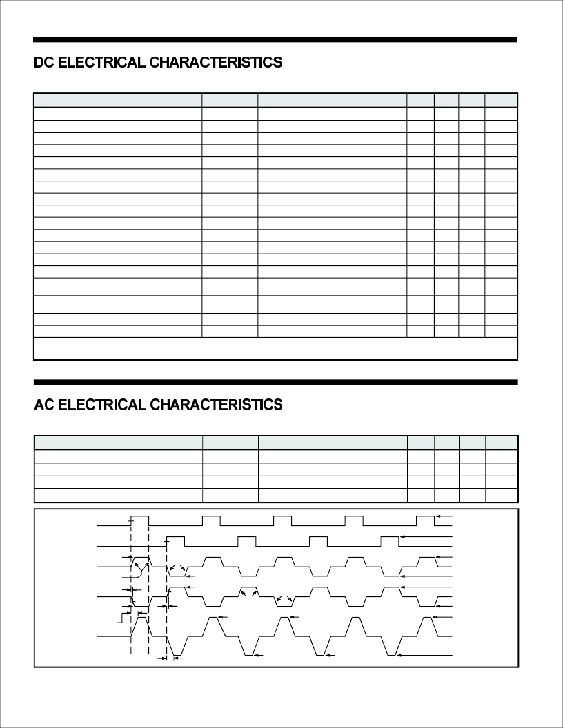
SYMBOL
t
C
C
t
C
C
t
C
C
t
C
C
PHL
A
B
REF
A
PARAMETER
B
B
OUT
OUT
CONDITION
MIN
TYP
MAX
UNITS
Rise Time (
,
)
=
= 75pF
See Figure 3.
1.0
2.0
μs
Fall Time (
,
)
=
= 75pF
See Figure 3.
1.0
2.0
μs
Propagtion Delay Input to Output
=
= 75pF
See Figure 3.
3.0
μs
Propagtion Delay Input to Output
=
= 75pF
See Figure 3.
3.0
μs
A
A
OUT
OUT
R
A
B
F
A
B
PLH
A
B
Figure 3.
SWITCHING WAVEFORMS
-9.5V to -10.5V
+9.5V to +10.5V
-4.75V to -5.25V
2.0V
0.5V
+4.75V to +5.25V
2.0V
0.5V
-4.75V to -5.25V
+4.75V to +5.25V
DATA (A) 0V
DATA (B) 0V
A
OUT
0V
B
OUT
0V
DIFFERENTIAL
OUTPUT 0V
(
A
OUT -
)
B
OUT
50%
50%
V
REF
ADJUST
BY
C
A
t
PHL
ADJUST
BY
C
A
-V
REF
50%
50%
t
PLH
t
R
+V
REF
-V
REF
ADJUST
BY
C
B
2V
REF
ADJUST
BY
C
B
t
F
-2V
RE
HIGH
NULL
LOW
NOTE: OUTPUTS UNLOADED
HI-8382, HI-8383
+V = +15V, -V = -15V, V = V
= +5.0V, T
= Operating Temperature Range (unless otherwise specified).
REF
A
HOLT INTEGRATED CIRCUITS
4
相關(guān)PDF資料 |
PDF描述 |
|---|---|
| HI-8382S | 256 MACROCELL 3.3 VOLT ISP CPLD - NOT RECOMMENDED for NEW DESIGN |
| HI-8382ST | ARINC 429 DIFFERENTIAL LINE DRIVER |
| HI-8382U | 256 MACROCELL 3.3 VOLT ISP CPLD - NOT RECOMMENDED for NEW DESIGN |
| HI-8383 | ARINC 429 DIFFERENTIAL LINE DRIVER |
| HI-8383CT | Line Driver |
相關(guān)代理商/技術(shù)參數(shù) |
參數(shù)描述 |
|---|---|
| HI-8382JT | 制造商:HOLTIC 制造商全稱:Holt Integrated Circuits 功能描述:ARINC 429 DIFFERENTIAL LINE DRIVER |
| HI-8382S | 制造商:Holt Integrated Circuits 功能描述:ARINC 429 Differential Line Driver 28-Pin CLLCC |
| HI-8382SM | 制造商:未知廠家 制造商全稱:未知廠家 功能描述:Line Driver |
| HI-8382SM-01 | 制造商:HOLTIC 制造商全稱:Holt Integrated Circuits 功能描述:ARINC 429 DIFFERENTIAL LINE DRIVER |
| HI-8382SM-02 | 制造商:未知廠家 制造商全稱:未知廠家 功能描述:Line Driver |
發(fā)布緊急采購,3分鐘左右您將得到回復(fù)。