- 您現(xiàn)在的位置:買賣IC網(wǎng) > PDF目錄371807 > HFA3726IN (HARRIS SEMICONDUCTOR) 3.3V 288-mc CPLD PDF資料下載
參數(shù)資料
| 型號: | HFA3726IN |
| 廠商: | HARRIS SEMICONDUCTOR |
| 元件分類: | 衰減器 |
| 英文描述: | 3.3V 288-mc CPLD |
| 中文描述: | 10 MHz - 400 MHz RF/MICROWAVE QUADRAPHASE MODEM |
| 文件頁數(shù): | 8/21頁 |
| 文件大小: | 162K |
| 代理商: | HFA3726IN |
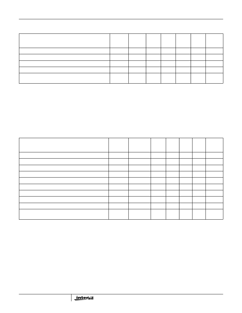
8
IF Demodulator RSSI Voltage Output Slope (Note 9)
Drssis
B
25
-
15
-
mV/dB
IF Demodulator RSSI DC Level, Pin = -30dBm (Note 9)
Drssi_30
A
Full
0.904
1.46
1.71
Vdc
IF Demodulator RSSI DC Level, Pin = -70dBm (Note 9)
Drssi_70
A
Full
0.456
0.86
0.99
Vdc
IF Demodulator RSSI Linear Dynamic Range (Note 10)
Drssidr
B
25
-
60
-
dB
IF Demodulator RSSI Rise and Fall Time from -30dBm to
-50dBm Input at 100pF Load
Drssitr
B
25
-
0.3
-
μ
s
NOTES:
6. A = Production Tested, B = Based on Characterization, C = By Design
7. 2XLO input = 572MHz, measure IF input level required to drop the I and Q output at 6MHz by 3dB from a reference output generated at IF input
= -30dBm (hard limiting). This is a noise limited case with a BW of 47MHz. Please refer to the Overall Device Description, IF limiter.
8. The residual DC voltage generated by the RSSI circuit due to a noise limited stage at the end of the chain with no IF input. IF port terminated
into 50
. Please referred to the Overall Device Description, IF limiter.
9. Both limiter RSSI current outputs are summed by 2 on chip 6k
resistors in parallel.
10. Range is defined where the indicated received input strength by the RSSI is
±
3dBm accurate.
AC Electrical Specifications, Modulator Performance
Application Targeting IEEE 802.11, V
CC
= 3V, Figure 22
Unless Otherwise Specified
PARAMETER
SYMBOL
(NOTE 11)
TEST
LEVEL
TEMP
(
o
C)
MIN
TYP
MAX
UNITS
IF Modulator I/Q Amplitude Balance (Note 12)
Mabal
B
25
-1.0
0
+1.0
dB
IF Modulator I/Q Phase Balance (Note 12)
Mphbal
B
25
-4.0
0
+4.0
Degrees
IF modulator SSB Output Power (Note 13)
Mssbpw
A
Full
-12
-7
-4
dBm
IF Modulator Side Band Suppression (Note 13)
Mssbss
A
Full
26
33
-
dBc
IF Mod Carrier Suppression (LO Buffer Enabled) (Note 13)
Mssbcs
A
Full
28
30
-
dBc
IF Mod Carrier Suppression (LO Buffer Disabled) (Note 13)
Mssbcs1
B
25
28
36
-
dBc
IF Modulator Output Noise Floor
Moutn0
B
25
-
-132
-
dBm/Hz
IF Modulator I/Q 3dB Cutoff (Note 14)
Msel3f
A
Full
6.83
7.7
8.57
MHz
IF Modulator Spread Spectrum Output Power (Note 15)
Mdsspw
B
25
-12
-7
-4
dBm
IF Modulator Side Lobe to Main Lobe Ratio, LPF = 7.7MHz
(Note 15)
Mdsssl
B
25
-
35
-
dB
NOTES:
11. A = Production Tested, B = Based on Characterization, C = By Design
12. Data is characterized by DC levels applied to MOD TXI and Q pins for 4 quadrants with LO output as reference or indirectly by the SSB
characteristics.
13. PoweratthefundamentalSSBfrequencyoftwo6MHz,90degreesapartsquarewavesappliedatTXIandTXQinputs.Levelsare3.4V
P-P
1.7Voffset.
14. Cutoff frequency is specified for both modulator and demodulator as the filter bank is shared and multiplexed for Transmit and Receive. Data is
characterized by observing the attenuation of the fundamental of a square wave digital input swept at each channel separately. The IF output
is down converted by an external wideband mixer with a coherent LO input for each of quadrature signals separately.
15. Typical ratio characterization with R
TUNE
set to 7.7MHz. TXI and TXQ analog Inputs at two independent and aligned 11M chip/s, 2
23
-1
sequence code signals.
AC Electrical Specifications, Demodulator Performance
Application Targeting IEEE 802.11, V
CC
= 3V, Figure 22
Unless Otherwise Specified
(Continued)
PARAMETER
SYMBOL
(NOTE 6)
TEST
LEVEL
TEMP
(
o
C)
MIN
TYP
MAX
UNITS
HFA3726
相關(guān)PDF資料 |
PDF描述 |
|---|---|
| HFA3765IA | AGC and Quadrature IF Demodulator |
| HFA3765 | AGC and Quadrature IF Demodulator |
| HFA3765IA96 | AGC and Quadrature IF Demodulator |
| HFA3766IN96 | 400MHz AGC Quadrature IF Modulator/Demodulator |
| HFA3766IN | 400MHz AGC Quadrature IF Modulator/Demodulator |
相關(guān)代理商/技術(shù)參數(shù) |
參數(shù)描述 |
|---|---|
| HFA3726IN WAF | 制造商:Harris Corporation 功能描述: |
| HFA3726IN96 | 制造商:Rochester Electronics LLC 功能描述:- Bulk |
| HFA3761 | 制造商:INTERSIL 制造商全稱:Intersil Corporation 功能描述:400MHz AGC and Quadrature IF Demodulator |
| HFA3761/3763IN WAF | 制造商:Harris Corporation 功能描述: |
| HFA3761IN | 制造商:INTERSIL 制造商全稱:Intersil Corporation 功能描述:400MHz AGC and Quadrature IF Demodulator |
發(fā)布緊急采購,3分鐘左右您將得到回復。