- 您現(xiàn)在的位置:買賣IC網(wǎng) > PDF目錄384398 > HE83139 (King Billion Electronics Co., Ltd.) 8-BIT MICRO-CONTROLLER PDF資料下載
參數(shù)資料
| 型號: | HE83139 |
| 廠商: | King Billion Electronics Co., Ltd. |
| 英文描述: | 8-BIT MICRO-CONTROLLER |
| 中文描述: | 8位微控制器 |
| 文件頁數(shù): | 2/9頁 |
| 文件大小: | 299K |
| 代理商: | HE83139 |
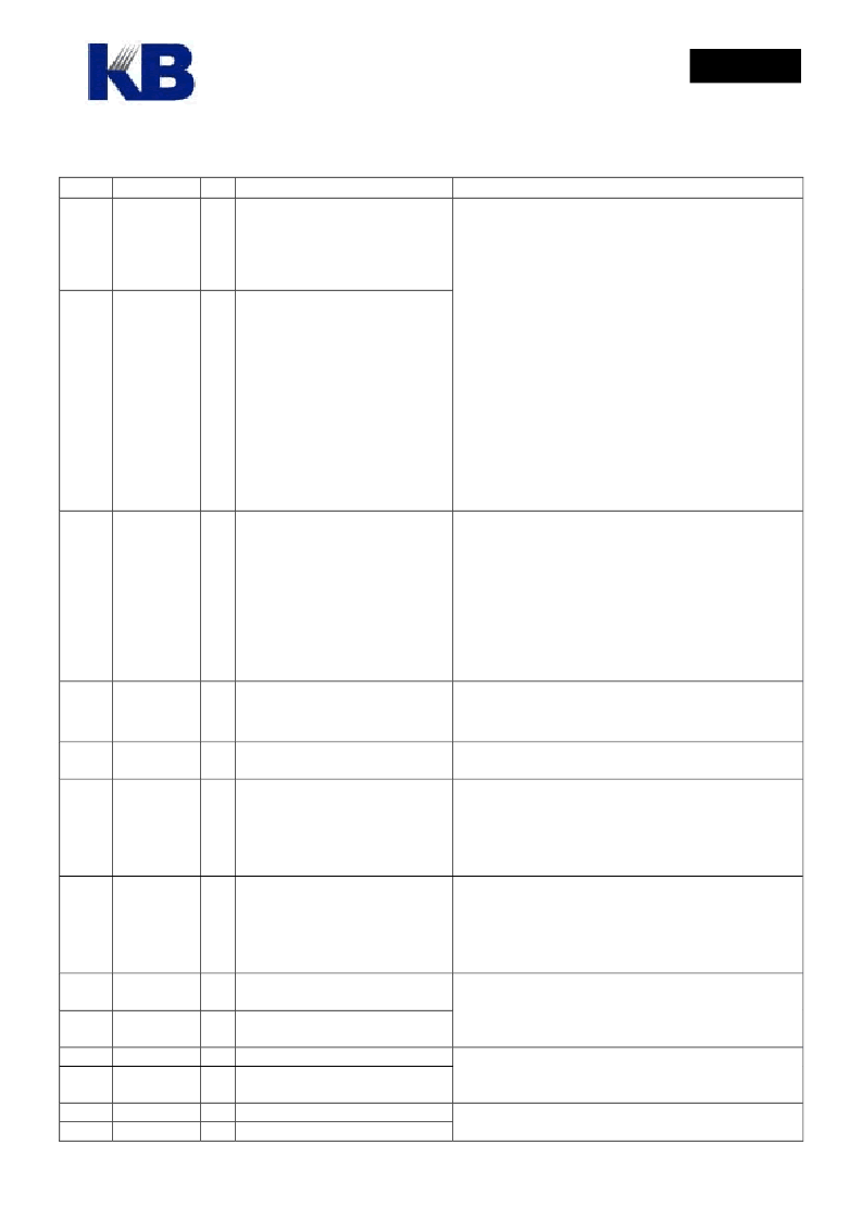
C. Pin Description
Pin #
Pin name I/O Function
KING BILLION ELECTRONICS CO., LTD
駿
億
電
子
股
份
有
限
公
司
HE83139
HE80000 SERIES
2
V1.0
Description
Mask Option setting:
MO_FCK/SCKN= 00 : Slow Clock only
78
77
FXI,
FXO
B,
O
External fast clock input/output
pins are used to connect crystal
or RC to generate the
32.768KHz ~ 8MHz system
clock.
81
80
SXI,
SXO
I,
O
External slow clock input/output
pins used to connect the
32.768KHz crystal to generate
slow clock for system operation
(slow mode), LCD display or
timer 1 clock source.
01 : Illegal
10
:
Dual Clock
11
:
Fast Clock only
MO_FOSCE= 0
:
Internal fast clock
1
:
External fast clock
MO_FXTAL= 0
:
R,C OSC. for Fast Clock
1
:
Crystal OSC. for Fast Clock
MO_SXTAL= 0
:
R,C OSC. for 32.768K Clock
1
:
Crystal OSC. for 32.768K Clock
。
Use OP1 and OP2 to switch among different
operation mode (NORMAL, SLOW, IDEL and
SLEEP). In Dual Clock mode, the main system clock
is still the Fast Clock. The 32768 Hz clock is for LCD
and Timer 1 only.
Active low and level trigger reset signal. User can
also set the mask option MO_PORE=1 to enable the
build-in Power-on reset circuit besides using the reset
pin.
Watch Dog Timer can also be enabled/disabled by the
mask option,
MO_WDTE = 0
:
Disable Watch Dog Timer
= 1
:
Enable Watch Dog Timer
Please bond this pin to ground by a 0 ohm
resistor to let it accessible when it’s necessary for
some testing.
76
RSTP_N
I System reset signal
79
TSTP_P
I IC Test Pin
91,92,
93,1
NC
No Connection Pin
83..
90
PRTD[7:0]
B
Bi-directional I/O port D. PRTD
[7:2] also used as wake-up pin,
and PRTD [7:6] also used as
external interrupt pin.
Mask options setting:
MO_DPP [7:0] = 1
:
Push-pull output.
= 0
:
Open-drain output.
Output must be “1” before reading whenever uses
them as input (Non tri-state structure).
Mask options setting:
MO_17PP [7:0] = 1
:
Push-pull output.
= 0
:
Open-drain output.
Output must be “1” before reading whenever uses
them as input (Non tri-state structure).
LCD common/segment driving pins.
LCD Data filled from 80H; please refer the LCD
RAM map.
When LV3=VDD, the charge pump
for LCD is turn off.
The capacitor between LC1 and LC2 shall be
removed to reduce power consumption.
12..19
PRT17[7:0]
B Bi-directional I/O port 17
11..4
52..59
COM[15:0]
O LCD COM Output
20..51
SEG[31:0]
O LCD SEG Output
61
60
LC2
LC1
B Charge Pump Switch 1
B Charge Pump Switch 2
63
62
LV3
LV1
B Charge Pump V3
B Charge Pump V1
Refer to application circuit.
相關(guān)PDF資料 |
PDF描述 |
|---|---|
| HE83141 | 8-BIT MICRO-CONTROLLER |
| HE83142 | 8-BIT MICRO-CONTROLLER |
| HE83143 | 8-BIT MICRO-CONTROLLER |
| HE83144 | 8-BIT MICRO-CONTROLLER |
| HE83145 | 8-BIT MICRO-CONTROLLER |
相關(guān)代理商/技術(shù)參數(shù) |
參數(shù)描述 |
|---|---|
| HE83139(S) | 制造商:未知廠家 制造商全稱:未知廠家 功能描述: |
| HE83141 | 制造商:KB 制造商全稱:KB 功能描述:8-BIT MICRO-CONTROLLER |
| HE83141(S) | 制造商:未知廠家 制造商全稱:未知廠家 功能描述: |
| HE83142 | 制造商:KB 制造商全稱:KB 功能描述:8-BIT MICRO-CONTROLLER |
| HE83142(S) | 制造商:未知廠家 制造商全稱:未知廠家 功能描述: |
發(fā)布緊急采購,3分鐘左右您將得到回復(fù)。