- 您現(xiàn)在的位置:買賣IC網(wǎng) > PDF目錄384395 > HCS11MS (INTERSIL CORP) Radiation Hardened Triple 3-Input AND Gate(抗輻射三3輸入與門) PDF資料下載
參數(shù)資料
| 型號: | HCS11MS |
| 廠商: | INTERSIL CORP |
| 元件分類: | 通用總線功能 |
| 英文描述: | Radiation Hardened Triple 3-Input AND Gate(抗輻射三3輸入與門) |
| 中文描述: | HC/UH SERIES, TRIPLE 3-INPUT AND GATE, UUC14 |
| 封裝: | 2.20 X 2.24 MM, DIE-14 |
| 文件頁數(shù): | 2/6頁 |
| 文件大小: | 160K |
| 代理商: | HCS11MS |
7-136
All Intersil semiconductor products are manufactured, assembled and tested under
ISO9000
quality systems certification.
Intersil products are sold by description only. Intersil Corporation reserves the right to make changes in circuit design and/or specifications at any time without
notice. Accordingly, the reader is cautioned to verify that data sheets are current before placing orders. Information furnished by Intersil is believed to be accurate
and reliable. However, no responsibility is assumed by Intersil or its subsidiaries for its use; nor for any infringements of patents or other rights of third parties which
may result from its use. No license is granted by implication or otherwise under any patent or patent rights of Intersil or its subsidiaries.
For information regarding Intersil Corporation and its products, see web site
http://www.intersil.com
Specifications HCS11MS
Absolute Maximum Ratings
Reliability Information
Supply Voltage . . . . . . . . . . . . . . . . . . . . . . . . . . . . . . -0.5V to +7.0V
Input Voltage Range, All Inputs . . . . . . . . . . . . .-0.5V to VCC +0.5V
DC Input Current, Any One Input
. . . . . . . . . . . . . . . . . . . . . . . .±
10mA
DC Drain Current, Any One Output
. . . . . . . . . . . . . . . . . . . . . . .±
25mA
(All Voltage Reference to the VSS Terminal)
Storage Temperature Range (TSTG). . . . . . . . . . . -65
o
C to +150
o
C
Lead Temperature (Soldering 10sec). . . . . . . . . . . . . . . . . . +265
o
C
Junction Temperature (TJ) . . . . . . . . . . . . . . . . . . . . . . . . . . +175
o
C
ESD Classification . . . . . . . . . . . . . . . . . . . . . . . . . . . . . . . . Class 1
Thermal Impedance . . . . . . . . . . . . . . . .
Weld Seal DIC. . . . . . . . . . . . . . . . . . .
Weld Seal Flat Pack . . . . . . . . . . . . . .
Power Dissipation per Package (PD)
For T
A
= -55
o
C to +100
o
C . . . . . . . . . . . . . . . . . . . . . . . . . . . . 1W
For T
A
= +100
o
C to +125
o
C Derate Linearly at 13mW/
o
C
θ
ja
θ
jc
75
o
C/W
64
o
C/W
16
o
C/W
12
o
C/W
CAUTION: As with all semiconductors, stress listed under “Absolute Maximum Ratings” may be applied to devices (one at a time) without resulting in permanent
damage. This is a stress rating only. Exposure to absolute maximum rating conditions for extended periods may affect device reliability. The conditions listed
under “Electrical Performance Characteristics” are the only conditions recommended for satisfactory device operation..
Operating Conditions
Supply Voltage . . . . . . . . . . . . . . . . . . . . . . . . . . . . . +4.5V to +5.5V
Input Rise and Fall Times at 4.5V VCC (TR, TF) . . . . . 100ns/V Max
Operating Temperature Range (T
A
) . . . . . . . . . . . . -55
o
C to +125
o
C
Input Low Voltage (VIL). . . . . . . . . . . . . . . . . . . 0.0V to 30% of VCC
Input High Voltage (VIH) . . . . . . . . . . . . . . . . . . 70% of VCC to VCC
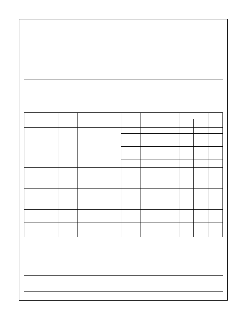
TABLE 1. DC. ELECTRICAL PERFORMANCE CHARACTERISTICS
PARAMETERS
SYMBOL
(NOTE 1)
CONDITIONS
GROUP
A SUB-
GROUPS
TEMPERATURE
LIMITS
UNITS
MIN
MAX
Quiescent Current
ICC
VCC = 5.5V,
VIN = VCC or GND
1
+25
o
C
-
10
μ
A
2, 3
+125
o
C, -55
o
C
-
200
μ
A
Output Current
(Sink)
IOL
VCC = 4.5V, VIH = 4.5V,
VOUT = 0.4V, VIL = 0V
1
+25
o
C
4.8
-
mA
2, 3
+125
o
C, -55
o
C
4.0
-
mA
Output Current
(Source)
IOH
VCC = 4.5V, VIH = 4.5V,
VOUT = VCC -0.4V,
VIL = 0V
1
+25
o
C
-4.8
-
mA
2, 3
+125
o
C, -55
o
C
-4.0
-
mA
Output Voltage Low
VOL
VCC = 4.5V, VIH = 3.15V,
IOL = 50
μ
A, VIL = 1.35V
1, 2, 3
+25
o
C, +125
o
C, -55
o
C
-
0.1
V
VCC = 5.5V, VIH = 3.85V,
IOL = 50
μ
A, VIL = 1.65V
1, 2, 3
+25
o
C, +125
o
C, -55
o
C
-
0.1
V
Output Voltage High
VOH
VCC = 4.5V, VIH = 3.15V,
IOH = -50
μ
A, VIL = 1.35V
1, 2, 3
+25
o
C, +125
o
C, -55
o
C
VCC
-0.1
-
V
VCC = 5.5V, VIH = 3.85V,
IOH = -50
μ
A, VIL = 1.65V
1, 2, 3
+25
o
C, +125
o
C, -55
o
C
VCC
-0.1
-
V
Input Leakage
Current
IIN
VCC = 5.5V, VIN = VCC or
GND
1
+25
o
C
-
±
0.5
μ
A
2, 3
+125
o
C, -55
o
C
-
±
5.0
μ
A
Noise Immunity
Functional Test
FN
VCC = 4.5V,
VIH = 0.70(VCC),
VIL = 0.30(VCC) (Note 2)
7, 8A, 8B
+25
o
C, +125
o
C, -55
o
C
-
-
-
NOTE:
1. All voltages reference to device GND.
2. For functional tests VO
≥
4.0V is recognized as a logic “1”, and VO
≤
0.5V is recognized as a logic “0”.
相關(guān)PDF資料 |
PDF描述 |
|---|---|
| HCS151D | Radiation Hardened 8-Input Multiplexer |
| HCS151K | Radiation Hardened 8-Input Multiplexer |
| HCS151MS | Radiation Hardened 8-Input Multiplexer |
| HCS151DMSR | Radiation Hardened 8-Input Multiplexer |
| HCS151HMSR | Radiation Hardened 8-Input Multiplexer |
相關(guān)代理商/技術(shù)參數(shù) |
參數(shù)描述 |
|---|---|
| HCS12 | 制造商:FREESCALE 制造商全稱:Freescale Semiconductor, Inc 功能描述:HCS12 Microcontrollers |
| HCS1201AX | 制造商:JLWORLD 制造商全稱:JLWORLD 功能描述:Electro-Magnetic Sound Generators |
| HCS1203AX | 制造商:JLWORLD 制造商全稱:JLWORLD 功能描述:Electro-Magnetic Sound Generators |
| HCS1206AX | 制造商:JLWORLD 制造商全稱:JLWORLD 功能描述:Electro-Magnetic Sound Generators |
| HCS1212AX | 制造商:JLWORLD 制造商全稱:JLWORLD 功能描述:Electro-Magnetic Sound Generators |
發(fā)布緊急采購,3分鐘左右您將得到回復(fù)。