- 您現(xiàn)在的位置:買賣IC網(wǎng) > PDF目錄370452 > HCPL-7720 40 ns Propagation Delay CMOS Optocoupler PDF資料下載
參數(shù)資料
| 型號(hào): | HCPL-7720 |
| 英文描述: | 40 ns Propagation Delay CMOS Optocoupler |
| 中文描述: | 40納秒的傳播延遲的CMOS光電耦合器 |
| 文件頁數(shù): | 8/18頁 |
| 文件大小: | 437K |
| 代理商: | HCPL-7720 |
8
Notes:
1. Absolute Maximum ambient operating
temperature means the device will not be
damaged if operated under these conditions.
It does not guarantee functionality.
2. The LED is ON when V
I
is low and OFF when
V
I
is high.
3. t
PHL
propagation delay is measured from the
50% level on the falling edge of the V
I
signal
to the 50% level of the falling edge of the V
O
signal. t
PLH
propagation delay is measured
from the 50% level on the rising edge of the
V
I
signal to the 50% level of the rising edge of
the V
signal.
4. PWD is defined as |t
PHL
- t
PLH
|.
%PWD(percent pulse width distortion) is
equal to the PWD divided by pulse width.
5. t
PSK
is equal to the magnitude of the worst
case difference in t
PHL
and/or t
PLH
that will
be seen between units at any given
temperature within the recommended
operating conditions.
6. CM
H
is the maximum common mode voltage
slew rate that can be sustained while
maintaining V
O
> 0.8 V
DD2
. CM
L
is the
maximum common mode voltage slew rate
that can be sustained while maintaining
V
O
< 0.8 V. The common mode voltage slew
rates apply to both rising and falling common
mode voltage edges.
7. Unloaded dynamic power dissipation is
calculated as follows: C
PD
* V
DD2
* f + I
DD
*
V
DD
, where f is switching frequency in MHz.
8. Device considered a two-terminal device:
pins 1, 2, 3, and 4 shorted together and pins
5, 6, 7, and 8 shorted together.
9. In accordance with UL1577, each HCPL-072X
is proof tested by applying an insulation test
voltage
≥
4500 V
RMS
for 1 second (leakage
detection current limit, I
I-O
≤
5
μ
A). Each
HCPL-772X is proof tested by applying an
insulation test voltage
≥
4500 Vrms for 1
second (leakage detection current limit.
I
I-O
≤
5
μ
A.)
10. The Input-Output Momentary Withstand
Voltage is a dielectric voltage rating that
should not be interpreted as an input-output
continuous voltage rating. For the continuous
voltage rating refer to your equipment level
safety specification or Agilent Application
Note 1074 entitled “Optocoupler Input-Output
Endurance Voltage.”
11. C
I
is the capacitance measured at pin 2 (V
I
).
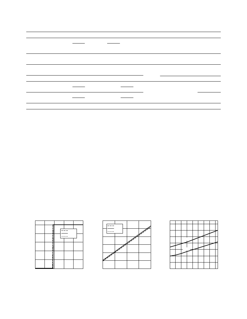
Figure 1. Typical output voltage vs. input
voltage.
Figure 2. Typical input voltage switching
threshold vs. input supply voltage.
Figure 3. Typical propagation delays vs.
temperature.
V
O
0
0
V
I
(V)
5
4
1
4
1
2
3
5
3
2
0
°
C
25
°
C
85
°
C
V
I
4.5
1.6
V
DD1
(V)
5.5
2.1
1.7
5.25
4.75
5
2.2
2.0
1.8
1.9
0
°
C
25
°
C
85
°
C
T
P
,
P
(
0
15
T
A
(C)
80
27
17
60
20
30
29
25
19
21
10
40
50
70
23
T
PLH
T
PHL
Package Characteristics
Parameter
Input-Output Momentary
Withstand Voltage
Symbol
V
ISO
Min.
3750
3750
Typ.
Max.
Units
Vrms
Test Conditions
RH
≤
50%,
t = 1 min.,
T
A
= 25
°
C
V
I-O
= 500 Vdc
Fig.
Note
8, 9,
10
072X
772X
Resistance
(Input-Output)
Capacitance
(Input-Output)
Input Capacitance
Input IC J unction-to-Case
Thermal Resistance
Output IC J unction-to-Case
Thermal Resistance
Package Power Dissipation
R
I-O
10
12
8
C
I-O
0.6
pF
f = 1 MHz
C
I
θ
jci
3.0
145
160
140
135
11
-772X
-072X
-772X
-072X
°
C/W
Thermocouple
located at center
underside of package
θ
jco
P
PD
150
mW
相關(guān)PDF資料 |
PDF描述 |
|---|---|
| HCPL-7721 | 40 ns Propagation Delay CMOS Optocoupler |
| HCPL-7840 | Isolation Amplifier(隔離放大器) |
| HCPL-7850 | Hermetically Sealed Analog Isolation Amplifier(密封模擬隔離放大器) |
| HCPL-7851 | Hermetically Sealed Analog Isolation Amplifier(密封模擬隔離放大器) |
| HCPL-7870 | Isolated 15-bit A/D Converter(隔離15位A/D轉(zhuǎn)換器) |
相關(guān)代理商/技術(shù)參數(shù) |
參數(shù)描述 |
|---|---|
| HCPL-7720#060 | 功能描述:高速光耦合器 1Ch 10mA 600mW RoHS:否 制造商:Avago Technologies 電流傳遞比: 最大波特率: 最大正向二極管電壓:1.75 V 最大反向二極管電壓:5 V 最大功率耗散:40 mW 最大工作溫度:+125 C 最小工作溫度:- 40 C 封裝 / 箱體:SOIC-5 封裝:Tube |
| HCPL-7720#300 | 功能描述:高速光耦合器 1Ch 10mA 600mW RoHS:否 制造商:Avago Technologies 電流傳遞比: 最大波特率: 最大正向二極管電壓:1.75 V 最大反向二極管電壓:5 V 最大功率耗散:40 mW 最大工作溫度:+125 C 最小工作溫度:- 40 C 封裝 / 箱體:SOIC-5 封裝:Tube |
| HCPL-7720#360 | 功能描述:高速光耦合器 1Ch 10mA 600mW RoHS:否 制造商:Avago Technologies 電流傳遞比: 最大波特率: 最大正向二極管電壓:1.75 V 最大反向二極管電壓:5 V 最大功率耗散:40 mW 最大工作溫度:+125 C 最小工作溫度:- 40 C 封裝 / 箱體:SOIC-5 封裝:Tube |
| HCPL-7720#500 | 功能描述:高速光耦合器 1Ch 10mA 600mW RoHS:否 制造商:Avago Technologies 電流傳遞比: 最大波特率: 最大正向二極管電壓:1.75 V 最大反向二極管電壓:5 V 最大功率耗散:40 mW 最大工作溫度:+125 C 最小工作溫度:- 40 C 封裝 / 箱體:SOIC-5 封裝:Tube |
| HCPL-7720#560 | 功能描述:高速光耦合器 1Ch 10mA 600mW RoHS:否 制造商:Avago Technologies 電流傳遞比: 最大波特率: 最大正向二極管電壓:1.75 V 最大反向二極管電壓:5 V 最大功率耗散:40 mW 最大工作溫度:+125 C 最小工作溫度:- 40 C 封裝 / 箱體:SOIC-5 封裝:Tube |
發(fā)布緊急采購,3分鐘左右您將得到回復(fù)。