- 您現(xiàn)在的位置:買賣IC網(wǎng) > PDF目錄223877 > HCPL-4504#300E (AGILENT TECHNOLOGIES INC) 1 CHANNEL LOGIC OUTPUT OPTOCOUPLER PDF資料下載
參數(shù)資料
| 型號: | HCPL-4504#300E |
| 廠商: | AGILENT TECHNOLOGIES INC |
| 元件分類: | 光電耦合器 |
| 英文描述: | 1 CHANNEL LOGIC OUTPUT OPTOCOUPLER |
| 封裝: | SURFACE MOUNT, DIP-8 |
| 文件頁數(shù): | 10/20頁 |
| 文件大?。?/td> | 303K |
| 代理商: | HCPL-4504#300E |
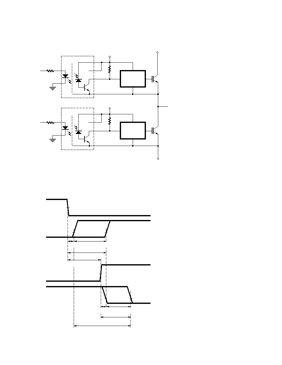
Figure 16. Typical Power Inverter.
Figure 17. LED Delay and Dead Time Diagram.
LED 1
OUT 1
LED 2
OUT 2
tPLH min
tPLH max
tPHL min
tPHL max
(tPLH max–tPLH min)
(tPHL max–tPHL min)
TURN-ON DELAY
MAXIMUM DEAD TIME
(tPLH max–tPLH min)
Power Inverter Dead
Time and Propagation
Delay Specifications
The HCPL-4504/0454/J454 and
HCNW4504 include a specifica-
tion intended to help designers
minimize “dead time” in their
power inverter designs. The new
“propagation delay difference”
specification (tPLH -tPHL) is useful
for determining not only how
much optocoupler switching delay
is needed to prevent “shoot-
through” current, but also for
determining the best achievable
worst-case dead time for a given
design.
When inverter power transistors
switch (Q1 and Q2 in Figure 17),
it is essential that they never
conduct at the same time.
Extremely large currents will flow
if there is any overlap in their
conduction during switching
transitions, potentially damaging
the transistors and even the sur-
rounding circuitry. This “shoot-
through” current is eliminated by
delaying the turn-on of one
transistor (Q2) long enough to
ensure that the opposing
transistor (Q1) has completely
turned off. This delay introduces a
small amount of “dead time” at
the output of the inverter during
which both transistors are off
during switching transitions.
Minimizing this dead time is an
important design goal for an
inverter designer.
The amount of turn-on delay
needed depends on the propaga-
tion delay characteristics of the
optocoupler, as well as the
characteristics of the transistor
base/gate drive circuit. Consider-
ing only the delay characteristics
of the optocoupler (the charac-
teristics of the base/gate drive
circuit can be analyzed in the
BASE/GATE
DRIVE CIRCUIT
HCPL-4504/0454/J454
HCNW4504
2
3
8
7
6
5
+HV
Q1
LED 1
OUT 1
BASE/GATE
DRIVE CIRCUIT
2
3
8
7
6
5
–HV
Q2
LED 2
OUT 2
+
HCPL-4504/0454/J454
HCNW4504
相關(guān)PDF資料 |
PDF描述 |
|---|---|
| HCPL-4504-300 | 1 CHANNEL LOGIC OUTPUT OPTOCOUPLER |
| HCPL-5501 | NPN-OUTPUT DC-INPUT OPTOCOUPLER |
| HCPL-5531 | Receptacle With No Tail |
| HCPL-573K | NPN-OUTPUT DC-INPUT OPTOCOUPLER |
| HCPL-6730 | Hermetically Sealed. Low IF. Wide Vcc. High Gain Optocouplers |
相關(guān)代理商/技術(shù)參數(shù) |
參數(shù)描述 |
|---|---|
| HCPL-4504-320E | 功能描述:高速光耦合器 1MBd 1Ch 12mA RoHS:否 制造商:Avago Technologies 電流傳遞比: 最大波特率: 最大正向二極管電壓:1.75 V 最大反向二極管電壓:5 V 最大功率耗散:40 mW 最大工作溫度:+125 C 最小工作溫度:- 40 C 封裝 / 箱體:SOIC-5 封裝:Tube |
| HCPL-4504-360E | 功能描述:高速光耦合器 1MBd 1Ch 12mA RoHS:否 制造商:Avago Technologies 電流傳遞比: 最大波特率: 最大正向二極管電壓:1.75 V 最大反向二極管電壓:5 V 最大功率耗散:40 mW 最大工作溫度:+125 C 最小工作溫度:- 40 C 封裝 / 箱體:SOIC-5 封裝:Tube |
| HCPL-4504-500E | 功能描述:高速光耦合器 1MBd 1Ch 12mA RoHS:否 制造商:Avago Technologies 電流傳遞比: 最大波特率: 最大正向二極管電壓:1.75 V 最大反向二極管電壓:5 V 最大功率耗散:40 mW 最大工作溫度:+125 C 最小工作溫度:- 40 C 封裝 / 箱體:SOIC-5 封裝:Tube |
| HCPL-4504-520E | 功能描述:高速光耦合器 1MBd 1Ch 12mA RoHS:否 制造商:Avago Technologies 電流傳遞比: 最大波特率: 最大正向二極管電壓:1.75 V 最大反向二極管電壓:5 V 最大功率耗散:40 mW 最大工作溫度:+125 C 最小工作溫度:- 40 C 封裝 / 箱體:SOIC-5 封裝:Tube |
| HCPL-4504-560E | 功能描述:高速光耦合器 1MBd 1Ch 12mA RoHS:否 制造商:Avago Technologies 電流傳遞比: 最大波特率: 最大正向二極管電壓:1.75 V 最大反向二極管電壓:5 V 最大功率耗散:40 mW 最大工作溫度:+125 C 最小工作溫度:- 40 C 封裝 / 箱體:SOIC-5 封裝:Tube |
發(fā)布緊急采購,3分鐘左右您將得到回復(fù)。