- 您現(xiàn)在的位置:買賣IC網(wǎng) > PDF目錄370451 > HCPL-316J 2.0 Amp Gate Drive Optocoupler with Integrated (V CE ) Desaturation Detection and Fault Status Feedback(帶集成不飽和檢測(cè)和誤差反饋的2.0 Amp門驅(qū)動(dòng)耦合器) PDF資料下載
參數(shù)資料
| 型號(hào): | HCPL-316J |
| 英文描述: | 2.0 Amp Gate Drive Optocoupler with Integrated (V CE ) Desaturation Detection and Fault Status Feedback(帶集成不飽和檢測(cè)和誤差反饋的2.0 Amp門驅(qū)動(dòng)耦合器) |
| 中文描述: | 2.0安培門極驅(qū)動(dòng)光電耦合器與集成(五長(zhǎng)官)飽和檢測(cè)與故障狀態(tài)反饋(帶集成不飽和檢測(cè)和誤差反饋的2.0安培門驅(qū)動(dòng)耦合器) |
| 文件頁(yè)數(shù): | 23/32頁(yè) |
| 文件大?。?/td> | 503K |
| 代理商: | HCPL-316J |
第1頁(yè)第2頁(yè)第3頁(yè)第4頁(yè)第5頁(yè)第6頁(yè)第7頁(yè)第8頁(yè)第9頁(yè)第10頁(yè)第11頁(yè)第12頁(yè)第13頁(yè)第14頁(yè)第15頁(yè)第16頁(yè)第17頁(yè)第18頁(yè)第19頁(yè)第20頁(yè)第21頁(yè)第22頁(yè)當(dāng)前第23頁(yè)第24頁(yè)第25頁(yè)第26頁(yè)第27頁(yè)第28頁(yè)第29頁(yè)第30頁(yè)第31頁(yè)第32頁(yè)
23
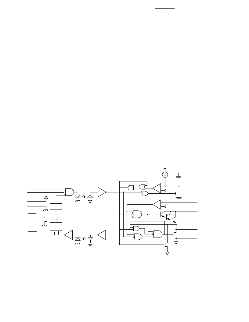
Behavioral Circuit
Schematic
The functional behavior of the
HCPL-316J is represented by the
logic diagram in Figure 64 which
fully describes the interaction and
sequence of internal and external
signals in the HCPL-316J.
Input IC
In the normal switching mode, no
output fault has been detected,
and the low state of the fault
latch allows the input signals to
control the signal LED. The fault
output is in the open-collector
state, and the state of the Reset
pin does not affect the control of
the IGBT gate. When a fault is
detected, the FAULT output and
Figure 64. Behavioral Circuit Schematic.
signal input are both latched. The
fault output changes to an active
low state, and the signal LED is
forced off (output LOW). The
latched condition will persist until
the Reset pin is pulled low.
Output IC
Three internal signals control the
state of the driver output: the
state of the signal LED, as well as
the UVLO and Fault signals. If no
fault on the IGBT collector is
detected, and the supply voltage
is above the UVLO threshold, the
LED signal will control the driver
output state. The driver stage
logic includes an interlock to
ensure that the pull-up and pull-
down devices in the output stage
are never on at the same time. If
an undervoltage condition is
detected, the output will be
actively pulled low by the 50x
DMOS device, regardless of the
LED state. If an IGBT
desaturation fault is detected
while the signal LED is on, the
Fault signal will latch in the high
state. The triple darlington AND
the 50x DMOS device are
disabled, and a smaller 1x DMOS
pull-down device is activated to
slowly discharge the IGBT gate.
When the output drops below two
volts, the 50x DMOS device again
turns on, clamping the IGBT gate
firmly to Vee. The Fault signal
remains latched in the high state
until the signal LED turns off.
V
IN+
(1)
V
IN–
(2)
V
CC1
(3)
GND (4)
FAULT (6)
RESET (5)
DELAY
R S
Q
FAULT
LED
12 V
+
–
V
CC2
(13)
7 V
–
+
DESAT (14)
V
E
(16)
250 μA
V
C
(12)
V
OUT
(11)
V
EE
(9,10)
50 x
1 x
F
UVLO
相關(guān)PDF資料 |
PDF描述 |
|---|---|
| HCPL-3700 | AC/DC to Logic Interface Optocouplers(AC/DC邏輯接口光耦合器) |
| HCPL-4100300 | Optically Coupled 20 mA Current Loop Transmitter |
| HCPL-4100500 | Optically Coupled 20 mA Current Loop Transmitter |
| HCPL4100 | Optically Coupled 20 mA Current Loop Transmitter |
| HCPL-4100 | Optically Coupled 20 mA Optically Coupled 20 mA |
相關(guān)代理商/技術(shù)參數(shù) |
參數(shù)描述 |
|---|---|
| HCPL-316J#500 | 功能描述:邏輯輸出光電耦合器 2.0A IGBT Gate Drive RoHS:否 制造商:Fairchild Semiconductor 絕緣電壓:4243 Vrms 輸出類型:Push-Pull 最大傳播延遲時(shí)間:500 ns 最大正向二極管電壓: 最大反向二極管電壓: 最大正向二極管電流: 最大連續(xù)輸出電流:2.5 A 最大功率耗散:100 mW 最大工作溫度:+ 100 C 最小工作溫度:- 40 C 封裝 / 箱體:SO-16 封裝:Tube |
| HCPL-316J-000E | 功能描述:邏輯輸出光電耦合器 2.0A IGBT Gate Drive RoHS:否 制造商:Fairchild Semiconductor 絕緣電壓:4243 Vrms 輸出類型:Push-Pull 最大傳播延遲時(shí)間:500 ns 最大正向二極管電壓: 最大反向二極管電壓: 最大正向二極管電流: 最大連續(xù)輸出電流:2.5 A 最大功率耗散:100 mW 最大工作溫度:+ 100 C 最小工作溫度:- 40 C 封裝 / 箱體:SO-16 封裝:Tube |
| HCPL-316J-000E | 制造商:Avago Technologies 功能描述:GATE DRIVE OPTOCOUPLERLF - LEAD FREE VE |
| HCPL-316J-500E | 功能描述:邏輯輸出光電耦合器 2.0A IGBT Gate Drive RoHS:否 制造商:Fairchild Semiconductor 絕緣電壓:4243 Vrms 輸出類型:Push-Pull 最大傳播延遲時(shí)間:500 ns 最大正向二極管電壓: 最大反向二極管電壓: 最大正向二極管電流: 最大連續(xù)輸出電流:2.5 A 最大功率耗散:100 mW 最大工作溫度:+ 100 C 最小工作溫度:- 40 C 封裝 / 箱體:SO-16 封裝:Tube |
| HCPL-3180 | 功能描述:高速光耦合器 2.0A IGBT Gate Drive RoHS:否 制造商:Avago Technologies 電流傳遞比: 最大波特率: 最大正向二極管電壓:1.75 V 最大反向二極管電壓:5 V 最大功率耗散:40 mW 最大工作溫度:+125 C 最小工作溫度:- 40 C 封裝 / 箱體:SOIC-5 封裝:Tube |
發(fā)布緊急采購(gòu),3分鐘左右您將得到回復(fù)。