- 您現(xiàn)在的位置:買賣IC網(wǎng) > PDF目錄385354 > HC5503CBZ96 (INTERSIL CORP) Low Cost 24V SLIC For PABX / Key Systems PDF資料下載
參數(shù)資料
| 型號(hào): | HC5503CBZ96 |
| 廠商: | INTERSIL CORP |
| 元件分類: | 模擬傳輸電路 |
| 英文描述: | Low Cost 24V SLIC For PABX / Key Systems |
| 中文描述: | TELECOM-SLIC, PDSO24 |
| 封裝: | GREEN, PLASTIC, MS-013AD, SOIC-24 |
| 文件頁數(shù): | 9/17頁 |
| 文件大?。?/td> | 386K |
| 代理商: | HC5503CBZ96 |

9
The Transversal Amplifier (TA)
Whereas the feed amplifiers perform the 4-wire to 2-wire
transmission function, the transversal amplifier acts as the
2-wire to 4-wire hybrid. The TA is a summing amplifier
configured to reject common mode signals. It will reject 2-
wire common mode signals. R
B1
and R
B2
act as loop
current sense resistors. The voice signal output of the
amplifier is a function of the differential voltages appearing
across R
B1
and R
B2
The transversal amplifier also has a DC output proportional
to the metallic current in the loop. The output voltage is
given by:
V
TX
= 2(I
TIP
+ I
RING
) (R
B1
+ R
B2
)
This DC level is used as an input to a comparator whose
output feeds into the logic circuitry as SH. This signal is used
to gate SHD output.
Voice signals on the loop are transformed by the TA into
ground referenced signals. Since the TA output has a DC
offset it is necessary to AC couple the output to any external
circuitry. Note, that during 4-wire to 2-wire transmission, the
transversal amplifier will have an audio signal at its output
proportional to the 4-wire audio receive signal and the loop’s
equivalent AC impedance. This is called the transhybrid
return, and must be cancelled (or balanced) out to prevent
an echo effect. Reference the Transhybrid Circuit section for
more information.
Loop Current Limiting
The maximum loop length for this application is a 533
load
across the feed amplifiers (24V
SUPPLY
- 8V
OVERHEAD
)/
30mA
MAX
loop current). However, on a short loop the line
resistance often approaches zero. Thus, a need exists to
control the maximum DC loop current that can flow around
the loop to prevent an excessive current drain from the
system battery. This limit is internally set to 30mA on the
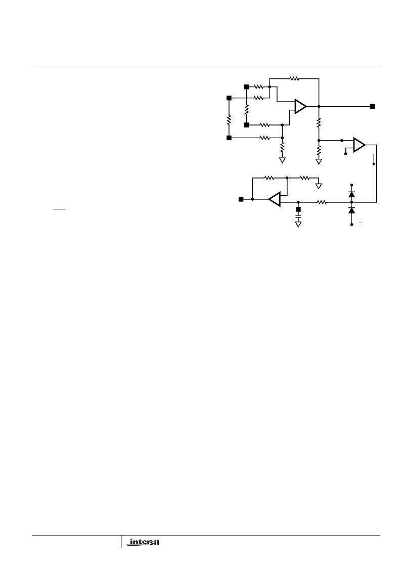
HC5503. Figure 3 depicts the feedback network that
modifies the V
RF
voltage as a function of metallic current.
Figure 4 illustrates the loop current characteristics as a
function of line resistance.
As indicated above, the TA has a DC voltage output
directly proportional to the loop current. This voltage level
is scaled by R
19
and R
18
. The scaled level forms the
‘Metallic’ input to one side of a Transconductance
Amplifier.
The reference input to this amplifier is generated in the bias
network, and is equivalent to 30mA. When the metallic input
exceeds the set reference level, the transconductance
amplifier sources current. This current will charge C
1
in
positive direction causing the V
RF
(Ring Feed) voltage to
approach the V
TF
(Tip Feed), effectively reducing the battery
feed across the loop which will limit the DC loop current. C
1
will continue to charge until an equilibrium level is attained at
I
LOOP
= I
LOOP
mA (Max). The time constant of this feedback
loop is set by R
21
(90k
) and C
1
which is nominally 0.33
μ
F.
The V
RF
voltage level is also modified to reduce or control
loop current during ring line faults (e.g., ground or power line
crosses), and thermal overload. Figure 8 illustrates this. The
thermal and fault current circuitry works in parallel with the
transconductance amplifier.
Longitudinal Amplifier
The longitudinal amplifier is an operational amplifier
configured as a closed loop differential amplifier with a
nominal gain of 0.1. The output is a measure of any
imbalance between I
TIP
and I
RING
. The transfer function of
this amplifier is given by:
V
LONG
= 0.1(I
TIP
- I
RING
) 150.
The gain factor is much less than one since ring voltage (up
to 150V
PEAK
) can appear at the Ring or Ring Feed Sense
terminals and are attenuated to avoid exceeding the
common mode range of the longitudinal amplifier’s input.
C
1
V
RF
V
TIP
R
B2
R
B1
V
RING
V
TF
TRANSVERSAL
AMP
V
TX
= -600 I
LOOP
V
B5
R
19
1.8K
R
18
90K
-4V
V
B
/2
KV
TX
FOR KV
TX
< V
B5
I
GM
> 0,
RING
FEED
90K
A
VCL
= 2
R
21
+
-
+
-
+
-
V
RF
V
TX
FIGURE 3. DC LOOP CURRENT CHARACTERISTICS
HC5503
相關(guān)PDF資料 |
PDF描述 |
|---|---|
| HC5503CCP | Bipolar Transistor; Collector Emitter Voltage, Vceo:50V; Transistor Polarity:NPN; Power Dissipation:900mW; DC Current Gain Min (hfe):180; Collector Current:500A; Package/Case:3-TO-92 |
| HC5503CCB | Unbalanced PBX/Key System SLIC, Subscriber Line Interface Circuit |
| HC5503TCB | Bipolar Transistor; Collector Emitter Voltage, Vceo:50V; Transistor Polarity:NPN; Power Dissipation:900mW; DC Current Gain Min (hfe):180; Collector Current:500A; Package/Case:3-TO-92 |
| HC5503TCP | Bipolar Transistor; Collector Emitter Voltage, Vceo:50V; Transistor Polarity:PNP; Power Dissipation:900mW; DC Current Gain Min (hfe):180; Collector Current:500A; Package/Case:3-TO-92 |
| HC5504B | EIA/ITU PABX SLIC with 40mA Loop Feed |
相關(guān)代理商/技術(shù)參數(shù) |
參數(shù)描述 |
|---|---|
| HC5503CCB | 制造商:Rochester Electronics LLC 功能描述:- Bulk |
| HC5503CCP | 制造商:Rochester Electronics LLC 功能描述:- Bulk |
| HC5503CM | 制造商:Rochester Electronics LLC 功能描述:- Bulk |
| HC5503CM96 | 制造商:未知廠家 制造商全稱:未知廠家 功能描述:Subscriber Line Interface Circuit |
| HC5503PRC | 制造商:INTERSIL 制造商全稱:Intersil Corporation 功能描述:Low Cost SLIC For Large Telecom Switches |
發(fā)布緊急采購,3分鐘左右您將得到回復(fù)。