- 您現(xiàn)在的位置:買賣IC網(wǎng) > PDF目錄370418 > HA17301P (Hitachi,Ltd.) 250000 SYSTEM GATE 1.5 VOLT FPGA PDF資料下載
參數(shù)資料
| 型號: | HA17301P |
| 廠商: | Hitachi,Ltd. |
| 英文描述: | 250000 SYSTEM GATE 1.5 VOLT FPGA |
| 中文描述: | 四路運(yùn)算放大器 |
| 文件頁數(shù): | 4/14頁 |
| 文件大小: | 61K |
| 代理商: | HA17301P |
HA17301P
4
HA17301P Application Examples
The HA17301P is a quad operational amplifier, and consists of four operational amplifier circuits and one
bias current circuit. The HA17301P features a wide operating temperature range, single-voltage power
supply operation, internal phase compensation, a wide zero-cross bandwidth, a low input bias current, and a
high open-loop gain. Thus the HA17301P can be used in a wide range of applications. This section
describes several applications using the HA17301P.
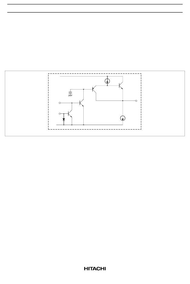
HA17301 Circuit Operation
V
CC
C
1
3 pF
Q
4
Q
5
Q
2
Q
10
Q
3
Q
1
D
1
GND
Op amp 1
Inverting input
3
Non inverting
input2
Output
4
Bias circuit
Figure 1 HA17301 Internal Equivalent Circuit
Figure 1 shows the internal equivalent circuit for the HA17301P bias circuit and one operational amplifier
circuit (Op amp 1).
Op amp 1 is basically an emitter ground type operational amplifier in which the input transistor Q
1
, the
buffer transistor Q
4
, the current source transistor Q
5
, the output emitter-follower transistor Q
2
, and the
current source transistor Q
10
form an inverting amplifier. The voltage gain of this circuit is all given by the
transistor Q
1
, and the adoption of the current-supply load Q
5
allows this circuit to provide a large open-loop
gain even at low power-supply voltages. Next, the emitter-follower transistor Q
2
lowers the output
impedance of this circuit. The use of the power-supply transistor Q
10
as the load for Q
2
gives this circuit an
extremely large dynamic range, and essentially an amplitude from ground to (V
CC
– 1) can be acquired.
Also, the buffer transistor Q
4
is used to reduce the input current without increasing the DC input voltage
level. Since the capacitor C
1
is used to preserve stability when this inverting amplifier is used as a closed
circuit, no external compensation is required.
Now consider the non inverting circuit. Assuming that the current amplification ratio provided by Q
3
is
adequately large for the current flowing into the non inverting input, then all that current will flow through
diode D
1
and the voltage drop induced in the diode D
1
by this input current will be applied to the Q
3
base-
emitter junction. Therefore, if D
1
and Q
3
are matched, a current equal to the input current will flow in the
Q
3
emitter. Assuming that the current amplification ratio provided by Q
3
is adequately large, a current equal
to the input current will flow in the Q
3
collector. This is called a “current mirror”, and when an external
feedback resistor is used, a current equal to the non inverting input current will flow in this resistor and thus
determine the output voltage.
相關(guān)PDF資料 |
PDF描述 |
|---|---|
| HA17324 | Quad Operational Amplifier |
| HA17324A | Quad Operational Amplifier |
| HA17384HPS | High Speed Current Mode PWM Control IC for Switching Power Supply(開關(guān)電源的高速電流模式PWM控制芯片) |
| HA17384SPS | High Speed Current Mode PWM Control IC for Switching Power Supply(開關(guān)電源的高速電流模式PWM控制芯片) |
| HA17385HRP | High Speed Current Mode PWM Control IC for Switching Power Supply(開關(guān)電源的高速電流模式PWM控制芯片) |
相關(guān)代理商/技術(shù)參數(shù) |
參數(shù)描述 |
|---|---|
| HA17324 | 制造商:HITACHI 制造商全稱:Hitachi Semiconductor 功能描述:Quad Operational Amplifier |
| HA17324/ASERIES | 制造商:未知廠家 制造商全稱:未知廠家 功能描述: |
| HA17324A | 制造商:HITACHI 制造商全稱:Hitachi Semiconductor 功能描述:Quad Operational Amplifier |
| HA17324AF | 制造商:未知廠家 制造商全稱:未知廠家 功能描述:Operational Amplifier |
| HA17324AF(EL-E) | 制造商:Renesas Electronics Corporation 功能描述: 制造商:Renesas Electronics Corporation 功能描述:OP Amp Quad GP 32V T/R |
發(fā)布緊急采購,3分鐘左右您將得到回復(fù)。