- 您現(xiàn)在的位置:買賣IC網(wǎng) > PDF目錄370395 > GT28F320D18B110 x16 Flash EEPROM PDF資料下載
參數(shù)資料
| 型號: | GT28F320D18B110 |
| 英文描述: | x16 Flash EEPROM |
| 中文描述: | x16閃存EEPROM |
| 文件頁數(shù): | 49/83頁 |
| 文件大小: | 836K |
| 代理商: | GT28F320D18B110 |
第1頁第2頁第3頁第4頁第5頁第6頁第7頁第8頁第9頁第10頁第11頁第12頁第13頁第14頁第15頁第16頁第17頁第18頁第19頁第20頁第21頁第22頁第23頁第24頁第25頁第26頁第27頁第28頁第29頁第30頁第31頁第32頁第33頁第34頁第35頁第36頁第37頁第38頁第39頁第40頁第41頁第42頁第43頁第44頁第45頁第46頁第47頁第48頁當(dāng)前第49頁第50頁第51頁第52頁第53頁第54頁第55頁第56頁第57頁第58頁第59頁第60頁第61頁第62頁第63頁第64頁第65頁第66頁第67頁第68頁第69頁第70頁第71頁第72頁第73頁第74頁第75頁第76頁第77頁第78頁第79頁第80頁第81頁第82頁第83頁
28F320D18
Product Preview
45
7.3.3
Using Asynchronous Page Mode
Upon power-up or return from reset, the device defaults to asynchronous page mode, with a page
size of four words. This read mode is only supported from the main blocks, and is not supported
from other locations within the device, such as the parameter blocks, the device identification
codes, query information, and status register.
In asynchronous page mode, CLK is ignored and ADV# must be held low throughout the page
access. With ADV# low, the internal address latch is open, allowing new page accesses. The initial
valid address will store four words of data in the internal page buffer. Each word is then output onto
the data lines by toggling address lines A
1-0
.
If an application only uses the asynchronous page mode capability, CLK and ADV# can be tied to
V
SS
, as shown in
Figure 20, “Different Clock Options” on page 48
. This shows an ideal, glueless
interface. If the processor does not provide any or all of these signals, some glue logic may be
required. More information on signal generation is covered later in this section. Grounding CLK
and ADV# will minimize the power consumed by these two pins and will simplify the interface,
making it compatible with standard flash memory and industry standard page mode ROMs. With
the ADV# signal tied low, the addresses cannot be latched into the device. This means that
addresses must stay valid throughout the entire read or write cycle, until CE# or either WE# or OE#
go high.
Figure 17, “Asynchronous Page Mode Read Waveform” on page 46
, shows an
asynchronous read timing diagram with ADV# held low. Note that address lines A
1-0
are toggled to
clock out the data.
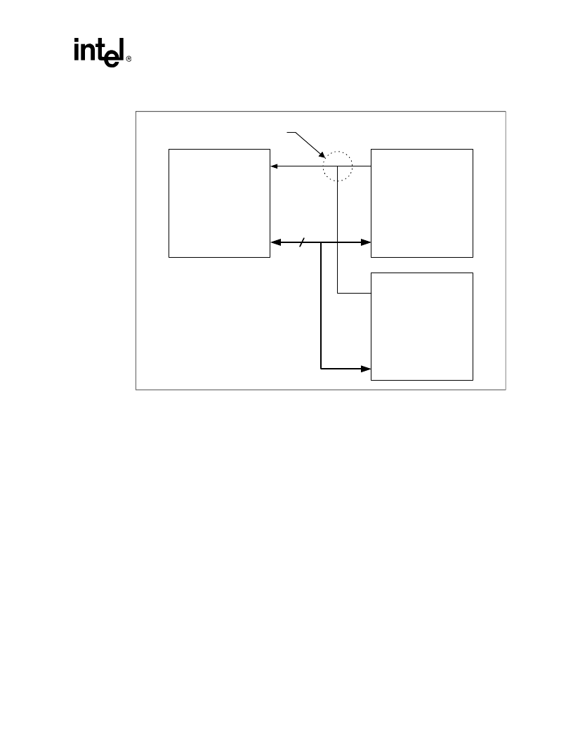
Figure 15. WAIT# Pin Connection Using Multiple Flash Memory Components
Burst CPU
or System
Wait-State Logic
1.8 Volt Dual-Plane
Flash Memory
WAIT#
1.8 Volt Dual-Plane
Flash Memory
WAIT#
READY#
Wire OR’d WAIT#
Data
DQ
15-0
DQ
15-0
x16
相關(guān)PDF資料 |
PDF描述 |
|---|---|
| GT28F320D18B120 | x16 Flash EEPROM |
| GT3-20DP-2.5DSA | Antenna, Sensor, and Communications Trunk Line Connections |
| GT3TK-36DP-DSA | Antenna, Sensor, and Communications Trunk Line Connections |
| GT3TK-48TP-DS | Antenna, Sensor, and Communications Trunk Line Connections |
| GT3-16DP-2.5DSA | Antenna, Sensor, and Communications Trunk Line Connections |
相關(guān)代理商/技術(shù)參數(shù) |
參數(shù)描述 |
|---|---|
| GT28F320D18B120 | 制造商:未知廠家 制造商全稱:未知廠家 功能描述:x16 Flash EEPROM |
| GT28F320S3-100 | 制造商:INTEL 制造商全稱:Intel Corporation 功能描述:WORD-WIDE FlashFile⑩ MEMORY FAMILY |
| GT28F320S3-120 | 制造商:INTEL 制造商全稱:Intel Corporation 功能描述:WORD-WIDE FlashFile MEMORY FAMILY |
| GT28F320W18BC60 | 制造商:INTEL 制造商全稱:Intel Corporation 功能描述:Intel? Wireless Flash Memory |
| GT28F320W18BC80 | 制造商:INTEL 制造商全稱:Intel Corporation 功能描述:Intel? Wireless Flash Memory |
發(fā)布緊急采購,3分鐘左右您將得到回復(fù)。