- 您現(xiàn)在的位置:買賣IC網(wǎng) > PDF目錄65272 > GSC93BC66 (GTM CORPORATION) Automotive Relays; V23076A1022D143 ( Tyco Electronics ) PDF資料下載
參數(shù)資料
| 型號: | GSC93BC66 |
| 廠商: | GTM CORPORATION |
| 英文描述: | Automotive Relays; V23076A1022D143 ( Tyco Electronics ) |
| 中文描述: | 2線串行EEPROM |
| 文件頁數(shù): | 5/8頁 |
| 文件大小: | 295K |
| 代理商: | GSC93BC66 |
GSC93BC46/56/66
Page: 5/8
ISSUED DATE :2006/06/14
REVISED DATE :
ERASE (ERASE): The Erase (ERASE) instruction clears the designated memory location to a logic ‘1’ state.
After the Op Code and address location is inputted, the chip will enter into an erase cycle. When the cycle
completes, the chip will automatically enter into standby mode.
WRITE (WRITE): The Write (WRITE) instruction is used to write to a specific memory location. If word mode
(x16) is selected, then 16 bits of data will be written into the location. If byte mode (x8) is chosen, then 8 bits of
data will be written into the location. The write cycle will begin automatically after the 8 or 16 bits are shifted
into the chip.
ERASE ALL (ERAL): The Erase All (ERAL) instruction is primarily used for testing purposes and only
functions when VCC=4.5V to 5.5V. This instruction will clear the entire memory array to ‘1’.
WRITE ALL (WRAL): The Write All (WRAL) instruction will program the entire memory array according to the 8
or 16-bit data pattern provided. The instruction will only be valid when VCC=4.5V to 5.5V.
ERASE/WRITE DISABLE (EWDS): The Erase/Write Disable (EWDS) instruction blocks any kind of erase or
program operations from modifying the contents of the memory array. This instruction should be executed after
erasing or programming to prevent accidental data loss.
Note also that the READ instruction will operate regardless of whether the chip is disabled from program and
write operations.
Ready/Busy
To determine whether the chip has completed an erase or write operation, the CS signal can be pulled LOW
for a minimum of 250ns (tCS) and then pulled back HIGH to enter Ready/Busy mode. If the chip is currently in
the programming cycle, tWP, then the DO pin will go low (logical “0”). When the write cycle completes, the DO
pin is pulled high (logical “1”) to indicate that the part can receive anther instruction. Note that the Ready/Busy
polling cannot be done if the chip has already finished and returned back to standby mode.
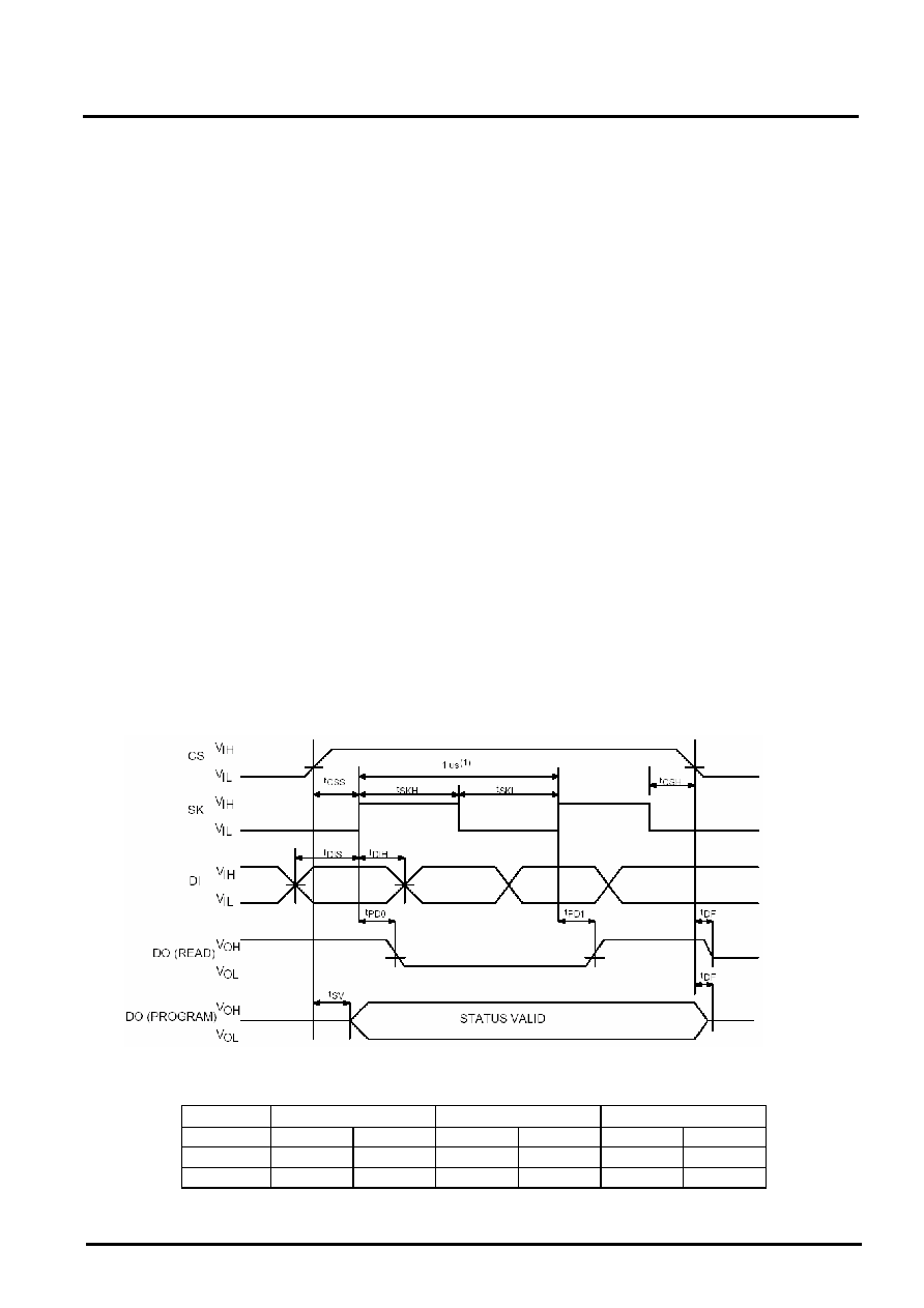
Timing Diagrams
Synchronous Data Timing
Note (1): This is the minimum SK period.
Organization Key for TIMING Diagrams
I/O
GSC93BC46(1K)
GSC93BC56(2K)
GSC93BC66(4K)
X8
X16
X8
X16
X8
X16
AN
A6
A5
A8(1)
A7(2)
A8
A7
DN
D7
D15
D7
D15
D7
D15
Note:
1. A8 is a DON’T CARE value, but the extra clock is required.
2. A7 is a DON’T CARE value, but the extra clock is required.
相關(guān)PDF資料 |
PDF描述 |
|---|---|
| GSC9431 | P-CHANNEL ENHANCEMENT MODE POWER MOSFET |
| GSC9435M | P-CHANNEL ENHANCEMENT MODE POWER MOSFET |
| GSC945 | Automotive Relays; V23133A1001C133 ( Tyco Electronics ) |
| GSC9563 | P-CHANNEL ENHANCEMENT MODE POWER MOSFET |
| GSC9575 | P-CHANNEL ENHANCEMENT MODE POWER MOSFET |
相關(guān)代理商/技術(shù)參數(shù) |
參數(shù)描述 |
|---|---|
| GSC9406 | 制造商:GTM 制造商全稱:GTM 功能描述:N-CHANNEL ENHANCEMENT MODE POWER MOSFET |
| GSC9410 | 制造商:GTM 制造商全稱:GTM 功能描述:N-CHANNEL ENHANCEMENT MODE POWER MOSFET |
| GSC9431 | 制造商:GTM 制造商全稱:GTM 功能描述:P-CHANNEL ENHANCEMENT MODE POWER MOSFET |
| GSC9435 | 制造商:GTM 制造商全稱:GTM 功能描述:P-CHANNEL ENHANCEMENT MODE POWER MOSFET |
| GSC9435M | 制造商:GTM 制造商全稱:GTM 功能描述:P-CHANNEL ENHANCEMENT MODE POWER MOSFET |
發(fā)布緊急采購,3分鐘左右您將得到回復(fù)。