- 您現(xiàn)在的位置:買賣IC網(wǎng) > PDF目錄223866 > GS8342D37BD-300I (GSI TECHNOLOGY) 1M X 36 QDR SRAM, 0.45 ns, PBGA165 PDF資料下載
參數(shù)資料
| 型號(hào): | GS8342D37BD-300I |
| 廠商: | GSI TECHNOLOGY |
| 元件分類: | SRAM |
| 英文描述: | 1M X 36 QDR SRAM, 0.45 ns, PBGA165 |
| 封裝: | 13 X 15 MM, 1 MM PITCH, FPBGA-165 |
| 文件頁(yè)數(shù): | 30/30頁(yè) |
| 文件大小: | 962K |
| 代理商: | GS8342D37BD-300I |
第1頁(yè)第2頁(yè)第3頁(yè)第4頁(yè)第5頁(yè)第6頁(yè)第7頁(yè)第8頁(yè)第9頁(yè)第10頁(yè)第11頁(yè)第12頁(yè)第13頁(yè)第14頁(yè)第15頁(yè)第16頁(yè)第17頁(yè)第18頁(yè)第19頁(yè)第20頁(yè)第21頁(yè)第22頁(yè)第23頁(yè)第24頁(yè)第25頁(yè)第26頁(yè)第27頁(yè)第28頁(yè)第29頁(yè)當(dāng)前第30頁(yè)
Preliminary
GS8342D07/10/19/37BD-450/400/350/333/300
Specifications cited are subject to change without notice. For latest documentation see http://www.gsitechnology.com.
Rev: 1.00 4/2011
9/30
2011, GSI Technology
FLXDrive-II Output Driver Impedance Control
HSTL I/O SigmaQuad-II+ SRAMs are supplied with programmable impedance output drivers. The ZQ pin must be connected to
VSS via an external resistor, RQ, to allow the SRAM to monitor and adjust its output driver impedance. The value of RQ must be
5X the value of the desired RAM output impedance. The allowable range of RQ to guarantee impedance matching continuously is
between 175
Ω and 350Ω. Periodic readjustment of the output driver impedance is necessary as the impedance is affected by drifts
in supply voltage and temperature. The SRAM’s output impedance circuitry compensates for drifts in supply voltage and
temperature. A clock cycle counter periodically triggers an impedance evaluation, resets and counts again. Each impedance
evaluation may move the output driver impedance level one step at a time towards the optimum level. The output driver is
implemented with discrete binary weighted impedance steps.
Input Termination Impedance Control
These SigmaQuad-II+ SRAMs are supplied with programmable input termination on Data (D), Byte Write (BW), and Clock (K/K)
input receivers. Input termination can be enabled or disabled via the ODT pin (6R). When the ODT pin is tied Low (or left
floating —the pin has a small pull-down resistor), input termination is disabled. When the ODT pin is tied High, input termination
is enabled. Termination impedance is programmed via the same RQ resistor (connected between the ZQ pin and VSS) used to
program output driver impedance, and is nominally RQ*0.6 Thevenin-equivalent when RQ is between 175
Ω and 250Ω. Periodic
readjustment of the termination impedance occurs to compensate for drifts in supply voltage and temperature, in the same manner
as for driver impedance (see above).
Note:
When ODT = 1, Data (D), Byte Write (BW), and Clock (K, K) input termination is always enabled. Consequently, D, BW, K, K
inputs should always be driven High or Low; they should never be tri-stated (i.e., in a High-Z state). If the inputs are tri-stated, the
input termination will pull the signal to VDDQ/2 (i.e., to the switch point of the diff-amp receiver), which could cause the receiver
to enter a meta-stable state and prevent the SRAM from operating within specification.
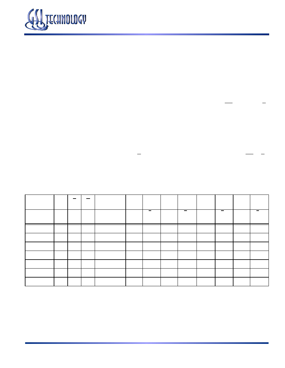
Separate I/O SigmaQuad II+ B4 SRAM Truth Table
Previous
Operation
A
R
W
Current
Operation
D
Q
K
↑
(tn-1)
K
↑
(tn)
K
↑
(tn)
K
↑
(tn)
K
↑
(tn)
K
↑
(tn+1)
K
↑
(tn+1)
K
↑
(tn+2)
K
↑
(tn+2)
K
↑
(tn+2)
K
↑
(tn+2)
K
↑
(tn+3)
K
↑
(tn+3)
Deselect
X
1
Deselect
X
—
Hi-Z
—
Write
X
1
X
Deselect
D2
D3
—
Hi-Z
—
Read
X
1
Deselect
X
—
Q2
Q3
—
Deselect
V
1
0
Write
D0
D1
D2
D3
Hi-Z
—
Deselect
V
0
X
Read
X
—
Q0
Q1
Q2
Q3
Read
V
X
0
Write
D0
D1
D2
D3
Q2
Q3
—
Write
V
0
X
Read
D2
D3
—
Q0
Q1
Q2
Q3
Notes:
1. “1” = input “high”; “0” = input “l(fā)ow”; “V” = input “valid”; “X” = input “don’t care”
2. “—” indicates that the input requirement or output state is determined by the next operation.
3. Q0, Q1, Q2, and Q3 indicate the first, second, third, and fourth pieces of output data transferred during Read operations.
4. D0, D1, D2, and D3 indicate the first, second, third, and fourth pieces of input data transferred during Write operations.
5. Users should not clock in metastable addresses.
相關(guān)PDF資料 |
PDF描述 |
|---|---|
| GS8342QT07BD-357 | 4M X 8 QDR SRAM, 0.45 ns, PBGA165 |
| GS8342QT10BGD-300T | 4M X 9 QDR SRAM, 0.45 ns, PBGA165 |
| GS8342TT06BGD-500T | 4M X 8 DDR SRAM, 0.45 ns, PBGA165 |
| GS841Z36CGT-166IT | 128K X 36 ZBT SRAM, 7 ns, PQFP100 |
| GS842Z18CB-250T | 256K X 18 ZBT SRAM, 5.5 ns, PBGA119 |
相關(guān)代理商/技術(shù)參數(shù) |
參數(shù)描述 |
|---|---|
| GS8342D38BD-350 | 制造商:GSI Technology 功能描述:165 FBGA - Bulk |
| GS8342D38BD-400 | 制造商:GSI Technology 功能描述:165 FBGA - Bulk |
| GS8342D38BD-450 | 制造商:GSI Technology 功能描述:165 FBGA - Bulk |
| GS8342D38BD-500 | 制造商:GSI Technology 功能描述:165 FBGA - Bulk |
| GS8342D38BD-550 | 制造商:GSI Technology 功能描述:165 FBGA - Bulk |
發(fā)布緊急采購(gòu),3分鐘左右您將得到回復(fù)。