- 您現(xiàn)在的位置:買賣IC網(wǎng) > PDF目錄64934 > FSO-211.059MHZAE1000 (FOX ELECTRONICS) CRYSTAL OSCILLATOR, CLOCK, 11.059 MHz, HCMOS/TTL OUTPUT PDF資料下載
參數(shù)資料
| 型號: | FSO-211.059MHZAE1000 |
| 廠商: | FOX ELECTRONICS |
| 元件分類: | XO, clock |
| 英文描述: | CRYSTAL OSCILLATOR, CLOCK, 11.059 MHz, HCMOS/TTL OUTPUT |
| 封裝: | J-LEADED, SMD, 4 PIN |
| 文件頁數(shù): | 1/2頁 |
| 文件大小: | 396K |
| 代理商: | FSO-211.059MHZAE1000 |
49
FOXElectronics 5570 Enterprise Parkway Fort Myers, Florida 33905 941-693-0099 FAX 941-693-1554
http://www.foxonline.com
1998 FOX ELECTRONICS
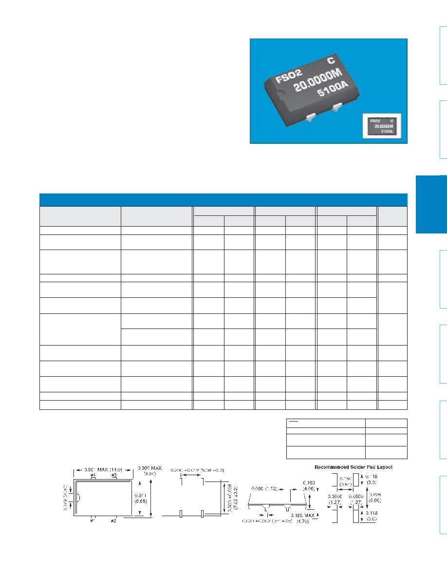
SURFACE MOUNT HCMOS CLOCK OSCILLATORS
FSO-2 SERIES
The FSO series is compatible with both TTL and HCMOS
technologies. The J-leaded configuration and high resistance to
soldering temperature make it ideal for surface mount production
processes. The FSO offers the low power consumption of HCMOS,
but will drive a full 10 TTL Gates when used in a TTL application.
This part is built to withstand vapor phase and other high temperature
soldering operations and to give long term outstanding performance
and reliability. Formechanically and electrically equivalent lower
cost alternative see page 50.
FEATURES
Extended Temperature Range
Solderable @ 260° for 10 sec.
Tape and Reel (1,000 pcs. STD)
Inch dimensions shall govern.
All dimensions are in inches & parenthetically in millimeters.
See page 63 for tape and reel specifications.
UNITS
MHz
PPM
C
V
mA
%
nS
V
mA
pF
TTL
mS
nS
ELECTRICAL CHARACTERISTICS (Ta = 25
°C, VDD = 5.0V, CL = Max Load)
MAX
66.667
+100
---
+70
+125
+5.5
35
20
60
---
7
0.4
4.0
-4.0
50
10
100
MIN
26.000+
-100
----
-10
-55
+4.5
40
---
4.6
MAX
66.667
+100
+200
+70
+125
+5.5
35
28
---
55
5
0.4
8
-0.4
5
10
100
MIN
26.000+
-100
-200
-10
-55
+4.5
---
45
2.4
FSO-2H
FSO-2T
FSO-2
* Inclusive of 25C tolerance, operating temperature range, input voltage change, load change, aging, shock, and vibration.
*** An internal pullup resistor from pin 1 to pin 4 allows active output if pin 1 is left open.
See page 35 for mechanical specifications, test circuits, and output waveform.
Note: ±50PPM frequency stability at -10 to +70°C also available (Up to 55 MHz)
Note: A 0.01F bypass capacitor should be placed between VDD (Pin 4) and GND (Pin 2) to minimize power supply line noise.
All specifications subject to change without notice.
Rev. 6/9/98
Actual Size
Pin Connections
#1 E/D**
#3 Output
#2 GND
#4 +5VDC
PARAMETERS
Frequency Range
Frequency Stability *
Temperature Range
Operating
(TOPR)
Storage
(TSTG)
Supply Voltage
(VDD)
Input Current
(IDD)
Output Symmetry
Rise Time
(TR)
Fall Time
(TF)
Output Voltage
(VOL)
(VOH)
Output Current
(IOL)
(IOH)
Output Load
Start-up Time
(TS)
Output Enable/Disable Time
MAX
26.000
+100
+200
+70
+125
+5.5
23
12
60
55
8
0.4
16
-0.4
50
10
4
100
MIN
1.025
-100
-200
-10
-55
+4.5
40
45
4.6
CONDITIONS
-10°C ~ +70°C
-40°C ~ +85°C
No Load
Output Disabled (IZ)
2.5V
1.4V
1.0V ~ 4.0V
0.4V ~ 2.4V
4.0V ~ 1.0V
2.4V ~ 0.4V
I= MAX
IOH = MAX
VOL = MAX
VOH = MIN
HCMOS
TTL
OSCILLA
T
O
R
S
OUTPUT (Pin 3)
ACTIVE
High Z
INH (Pin 1)
OPEN ***
'1' Level VIH ≥ 2.0 V (FSO-2 / FSO-2H)
'1' Level VIH ≥ 3.5 V (FSO-2 T)
'0' Level VIL ≤ 0.8 V (FSO-2 / FSO-2H)
'0' Level VIL ≤ 1.5 V (FSO-2 T)
ENABLE / DISABLE FUNCTION **
相關(guān)PDF資料 |
PDF描述 |
|---|---|
| FSO-2 | SPECIALTY ANALOG CIRCUIT, DSO4 |
| FSPLH1710SA | PLL FREQUENCY SYNTHESIZER, 1880 MHz, DSO22 |
| FSPLL870SA | PLL FREQUENCY SYNTHESIZER, 960 MHz, DSO22 |
| FSPLH1850SA | PLL FREQUENCY SYNTHESIZER, 1990 MHz, DSO22 |
| FSPLL824SA | PLL FREQUENCY SYNTHESIZER, 894 MHz, DSO22 |
相關(guān)代理商/技術(shù)參數(shù) |
參數(shù)描述 |
|---|---|
| FSO-2-18.4320MHZ | 制造商:FOX 功能描述: 制造商:Fox Electronics 功能描述: |
| FSO-2-24.0000MHZ | 制造商:FOX 功能描述: 制造商:Fox Electronics 功能描述: |
| FSO-2-24.0MHZ | 功能描述:標(biāo)準(zhǔn)時鐘振蕩器 REORD 559-KFO-2400 SMD CLK OSC 24.000 RoHS:否 制造商:AVX 產(chǎn)品:Standard Clock Oscillators 封裝 / 箱體:7 mm x 5 mm 頻率:75 MHz 頻率穩(wěn)定性:50 PPM 電源電壓:2.5 V 負(fù)載電容: 端接類型:SMD/SMT 最小工作溫度:0 C 最大工作溫度:+ 70 C 輸出格式:LVDS 尺寸: 封裝:Reel 系列: |
| FSO-2-3.6864MHZ | 制造商:Fox Electronics 功能描述: |
| FSO2-32 | 功能描述:標(biāo)準(zhǔn)時鐘振蕩器 32MHz RoHS:否 制造商:AVX 產(chǎn)品:Standard Clock Oscillators 封裝 / 箱體:7 mm x 5 mm 頻率:75 MHz 頻率穩(wěn)定性:50 PPM 電源電壓:2.5 V 負(fù)載電容: 端接類型:SMD/SMT 最小工作溫度:0 C 最大工作溫度:+ 70 C 輸出格式:LVDS 尺寸: 封裝:Reel 系列: |
發(fā)布緊急采購,3分鐘左右您將得到回復(fù)。