- 您現(xiàn)在的位置:買賣IC網(wǎng) > PDF目錄382969 > FS8170 (Electronic Theatre Controls, Inc.) 2.5 GHz Low Power Phase-locked Loop IC PDF資料下載
參數(shù)資料
| 型號(hào): | FS8170 |
| 廠商: | Electronic Theatre Controls, Inc. |
| 英文描述: | 2.5 GHz Low Power Phase-locked Loop IC |
| 中文描述: | 2.5 GHz的低功耗鎖相環(huán)集成電路 |
| 文件頁數(shù): | 10/17頁 |
| 文件大小: | 269K |
| 代理商: | FS8170 |

FS8170
Page 10
May 2003
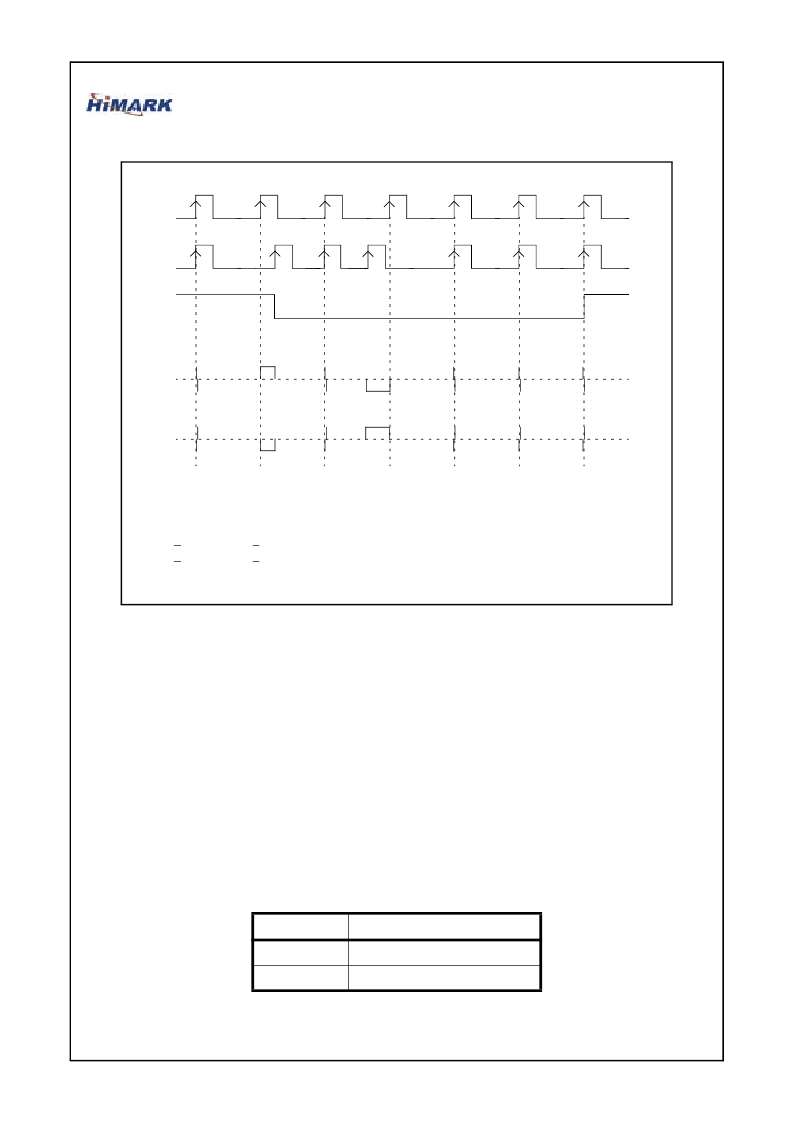
Fig. 3 – Phase comparator output waveforms
Charge Pump (CP)
The phase error signal, DO, generated from the PFD will pump charge into an external
loop filter, which then converts the charge to produce the VCO’s tuning voltage. With a
constant pumping rate, the shift of the VCO’s tuning voltage will be directly proportional
to the phase error signal DO. Two pumping rates, 1.5 mA and 6 mA, are provided by the
chip and are selectable through the bit CS as defined previously in Table 5. Also, the
charge pump characteristics corresponding to both modes are shown in the Typical Char-
acteristics section. The internal charge pump may be turned off by the pin ZC. When ZC
is set low, the internal charge pump will stay in its high-impedance state and will not pump
any charge into the external LPF. In this case, the user is allowed to utilize one’s own
charge pump by two control pins
φ
P and
φ
R which are defined in Table 6.
φ
P and
φ
R are
the error signals directly proportional to the positive/negative phase error when FC = “H.”
When FC = “L,” the relation becomes negative/positive.
Table 7: Setting for the pin ZC
ZC
Do Output
H
Normal output
L
High impedance
f
R
f
V
DO
LD
[FC=”H”]
DO
[FC=”L”]
1.
2.
Pulses of finite width on DO output are generated during locked state to prevent dead zone.
A “l(fā)ocked” condition (LD is HIGH) is indicated when the phase error is less than t1 or t2 at least for
3 consecutive comparison cycles, otherwise an “unlocked” condition (LD is LOW) is indicated.
The values of t
1
and t
2
depend on the XIN input frequency:
t
1
> 2/fosc (e.g. t
1
> 250 ns, if f
XIN
= 8 MHz)
t
2
> 2/fosc (e.g. t
2
> 250 ns, if f
XIN
= 8 MHz)
LD becomes HIGH during power-down mode (when EN is set LOW).
3.
4.
相關(guān)PDF資料 |
PDF描述 |
|---|---|
| FSLC-C160W | 1.5-2.0GHz Band Chip Multilayer 90deg.3dB Splitter |
| FSMD005-1206 | Surface Mount PTC FSMD1206 Series |
| FSMD010-1206 | Surface Mount PTC FSMD1206 Series |
| FSMD020-1206 | Surface Mount PTC FSMD1206 Series |
| FSMD035-1206 | Surface Mount PTC FSMD1206 Series |
相關(guān)代理商/技術(shù)參數(shù) |
參數(shù)描述 |
|---|---|
| FS8308 | 制造商:未知廠家 制造商全稱:未知廠家 功能描述:FRS. Pager. Multi-Channel system |
| FS85 | 制造商:Cooper Wiring Devices 功能描述: |
| FS850 | 制造商:Hubbell Wiring Device-Kellems 功能描述:FLUOR STARTER, 90/100W |
| FS-8502 | 制造商:PS 功能描述:FOR 85,90, AND 100WATT LAMPS |
| FS85-4 | 制造商:Cooper Wiring Devices 功能描述: |
發(fā)布緊急采購(gòu),3分鐘左右您將得到回復(fù)。