- 您現(xiàn)在的位置:買賣IC網(wǎng) > PDF目錄375777 > FDMS9600S (FAIRCHILD SEMICONDUCTOR CORP) Dual N-Channel PowerTrench㈢ MOSFET PDF資料下載
參數(shù)資料
| 型號: | FDMS9600S |
| 廠商: | FAIRCHILD SEMICONDUCTOR CORP |
| 元件分類: | 小信號晶體管 |
| 英文描述: | Dual N-Channel PowerTrench㈢ MOSFET |
| 中文描述: | 16 mA, 30 V, 2 CHANNEL, N-CHANNEL, Si, SMALL SIGNAL, MOSFET |
| 封裝: | ROHS COMPLIANT, POWER 56, 8 PIN |
| 文件頁數(shù): | 1/9頁 |
| 文件大小: | 336K |
| 代理商: | FDMS9600S |
F
M
2007 Fairchild Semiconductor Corporation
FDMS9600S Rev.D
www.fairchildsemi.com
1
tm
June 2007
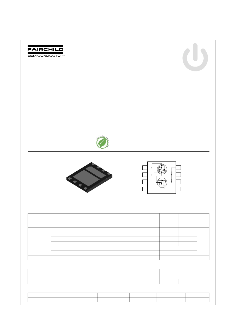
FDMS9600S
Dual N-Channel PowerTrench
MOSFET
Q1: 30V, 32A, 8.5m
Q2: 30V, 30A, 5.5m
Features
Q1: N-Channel
Max r
DS(on)
= 8.5m
at V
GS
= 10V, I
D
= 12A
Max r
DS(on)
= 12.4m
at V
GS
= 4.5V, I
D
= 10A
Q2: N-Channel
Max r
DS(on)
= 5.5m
at V
GS
= 10V, I
D
= 16A
Max r
DS(on)
= 7.0m
at V
GS
= 4.5V, I
D
= 14A
Low Qg high side MOSFET
Low r
DS(on)
low side MOSFET
Thermally efficient dual Power 56 package
Pinout optimized for simple PCB design
RoHS Compliant
General Description
This device includes two specialized MOSFETs in a unique dual
Power 56 package. It is designed to provide an optimal
Synchronous Buck power stage in terms of efficiency and PCB
utilization. The low switching loss "High Side" MOSFET is com-
plemented by a Low Conduction Loss "Low Side" SyncFET.
Applications
Synchronous Buck Converter for:
Notebook System Power
General Purpose Point of Load
MOSFET Maximum Ratings
T
A
= 25°C unless otherwise noted
Thermal Characteristics
Package Marking and Ordering Information
Symbol
V
DS
V
GS
Parameter
Q1
30
±20
32
55
12
60
Q2
30
±20
30
108
16
60
Units
V
V
Drain to Source Voltage
Gate to Source Voltage
Drain Current -Continuous (Package limited) T
C
= 25°C
-Continuous (Silicon limited) T
C
= 25°C
-Continuous T
A
= 25°C (Note 1a)
-Pulsed
Power Dissipation for Single Operation (Note 1a)
(Note 1b)
Operating and Storage Junction Temperature Range
I
D
A
P
D
2.5
1.0
W
T
J
, T
STG
-55 to +150
°
C
R
θ
JA
R
θ
JA
R
θ
JC
Thermal Resistance, Junction to Ambient (Note 1a)
Thermal Resistance, Junction to Ambient (Note 1b)
Thermal Resistance, Junction to Case
50
120
°C/W
3
1.2
Device Marking
FDMS9600S
Device
FDMS9600S
Package
Power 56
Reel Size
13”
Tape Width
12mm
Quantity
3000 units
G1
D1
D1
D1
S1/D2
S2
S2
Power 56
D1
G2S2
4
3
2
1
5
6
7
8
Q
1
Q2
相關(guān)PDF資料 |
PDF描述 |
|---|---|
| FDMS9620S | Dual N-Channel PowerTrench㈢ MOSFET Q1: 30V, 16A, 21.5mヘ Q2: 30V, 18A, 13mヘ |
| FDMW2512NZ | Monolithic Common Drain N-Channel 2.5V Specified PowerTrench MOSFET |
| FDN302 | P-Channel 2.5V Specified PowerTrench MOSFET |
| FDN302P | CAP CER 2.2UF 16V 10% X5R 1206 |
| FDN304PZ | P-Channel 1.8V Specified PowerTrench MOSFET |
相關(guān)代理商/技術(shù)參數(shù) |
參數(shù)描述 |
|---|---|
| FDMS9600S_08 | 制造商:FAIRCHILD 制造商全稱:Fairchild Semiconductor 功能描述:Dual N-Channel PowerTrench㈢ MOSFET |
| FDMS9620S | 功能描述:MOSFET 30V Dual N-Ch PowerTrench? MOSFET RoHS:否 制造商:STMicroelectronics 晶體管極性:N-Channel 汲極/源極擊穿電壓:650 V 閘/源擊穿電壓:25 V 漏極連續(xù)電流:130 A 電阻汲極/源極 RDS(導(dǎo)通):0.014 Ohms 配置:Single 最大工作溫度: 安裝風格:Through Hole 封裝 / 箱體:Max247 封裝:Tube |
| FDMS9620S_07 | 制造商:FAIRCHILD 制造商全稱:Fairchild Semiconductor 功能描述:Dual N-Channel PowerTrench㈢ MOSFET |
| FDMW2512NZ | 功能描述:MOSFET 2.5V NCH MONOLITHIC COMON DR RoHS:否 制造商:STMicroelectronics 晶體管極性:N-Channel 汲極/源極擊穿電壓:650 V 閘/源擊穿電壓:25 V 漏極連續(xù)電流:130 A 電阻汲極/源極 RDS(導(dǎo)通):0.014 Ohms 配置:Single 最大工作溫度: 安裝風格:Through Hole 封裝 / 箱體:Max247 封裝:Tube |
| FDN 304P | 制造商:Fairchild Semiconductor 功能描述:Bulk |
發(fā)布緊急采購,3分鐘左右您將得到回復(fù)。