- 您現(xiàn)在的位置:買賣IC網(wǎng) > PDF目錄375726 > FAN6520AIMX (FAIRCHILD SEMICONDUCTOR CORP) Single Synchronous Buck PWM Controller PDF資料下載
參數(shù)資料
| 型號: | FAN6520AIMX |
| 廠商: | FAIRCHILD SEMICONDUCTOR CORP |
| 元件分類: | 穩(wěn)壓器 |
| 英文描述: | Single Synchronous Buck PWM Controller |
| 中文描述: | 1 A SWITCHING CONTROLLER, 340 kHz SWITCHING FREQ-MAX, PDSO8 |
| 封裝: | MS-012AA, SOIC-8 |
| 文件頁數(shù): | 8/15頁 |
| 文件大小: | 580K |
| 代理商: | FAN6520AIMX |

8
REV. 1.0.2 8/26/04
FAN6520A
PRODUCT SPECIFICATION
Feedback Compensation
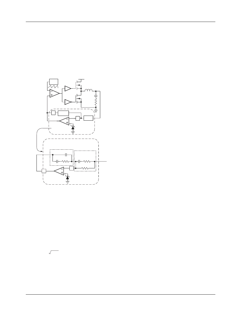
Figure 7 highlights the voltage-mode control loop for a
synchronous-rectified buck converter. The output voltage
(V
OUT
) is regulated to the reference voltage level. The error
amplifier (Error Amp) output (V
E/A
) is compared with the
oscillator (OSC) triangular wave to provide a pulse-width
modulated (PWM) wave with an amplitude of V
IN
at the SW
node. The PWM wave is smoothed by the output LC
filter (L
OUT
and C
OUT
).
Figure 7. Voltage Mode Buck
Converter Compensation Design
The modulator transfer function is the small-signal transfer
function of V
OUT
/V
COMP
. This function is dominated by a
DC Gain and the output filter (L
OUT
and C
OUT
), with a
double pole break frequency at F
LC
and a zero at F
ESR
.
The DC Gain of the modulator is simply the input voltage
(V
IN
) divided by the peak-to-peak oscillator voltage
V
OSC
.
The following equations define the modulator break
frequencies as a function of the output LC filter:
1.
The compensation network consists of the error ampli-
fier (internal to the FAN6520A) and the impedance
networks Z
IN
and Z
FB
. The goal of the compensation
network is to provide a closed loop transfer function
with the highest 0dB crossing frequency (F
0dB
) and
adequate phase margin. Phase margin is the difference
between the closed loop phase at F
0dB
and 180 degrees.
The equations below relate the compensation network’s
poles, zeros and gain to the components (R1, R2, R3,
C1, C2, and C3) in Figure 7.
Use the following steps to locate the poles and zeros of the
compensation network:
2.
Pick gain (R2/R1) for the desired converter bandwidth.
Place 1
st
zero below the filter’s double pole (~75% F
LC
).
Place 2
nd
zero at filter’s double pole.
Place 1
st
pole at the ESR zero.
Place 2
nd
pole at half the switching frequency.
3.
4.
5.
6.
7.
Check gain against the error amplifier’s open-loop gain.
8.
Estimate phase margin. Repeat if necessary.
Figure 8 shows an asymptotic plot of the DC-DC converter’s
gain vs. frequency. The actual Modulator Gain has a high
gain peak due to the high Q factor of the output filter and is
not shown in Figure 8. Using the above guidelines should
give a Compensation Gain similar to the curve plotted.
The open loop error amplifier gain bounds the compensation
gain. Check the compensation gain at FP2 with the capabili-
ties of the error amplifier. The Closed Loop Gain is con-
structed on the graph of Figure 8 by adding the Modulator
Gain (in dB) to the Compensation Gain (in dB). This is
equivalent to multiplying the modulator transfer function by
the compensation transfer function and plotting the gain.
The compensation gain uses external impedance networks
Z
FB
and Z
IN
to provide a stable, high bandwidth (BW)
overall loop. A stable control loop has a gain crossing with a
–20dB/decade slope and a phase margin greater than 45°.
Include worst case component variations when determining
phase margin.
Z
FB
COMP
FB
+V
OUT
Q2
L
OUT
C
OUT
+5V
VIN
SW
E
0.8V
ERROR
AMP
PWM
OSC
DETAILED COMPENSATION
COMPONENTS
COMP
FB
0.8V
ERROR
AMP
C1
R2
C3
R3
C2
R1
Z
IN
V
OUT
Z
FB
Z
IN
F
LC
2
π
L
C
×
-----------1
=
(15)
F
ESR
π
ESR
×
C
×
2
=
(16)
F
Z1
π
R
2
C
1
2
=
(17)
F
P1
2
π
R
2
C
C
1
+
+
C
2
C
-------------------1
=
(18)
F
Z2
π
C
3
R
1
π
R
3
C
3
R
3
(
)
2
=
(19)
F
P2
2
=
(20)
相關(guān)PDF資料 |
PDF描述 |
|---|---|
| FAN6520AM | Single Synchronous Buck PWM Controller |
| FAN6520AMX | Single Synchronous Buck PWM Controller |
| FAN6550M | |
| FAN6550MX | |
| FAN6550 | 2A DDR Bus Termination Regulator |
相關(guān)代理商/技術(shù)參數(shù) |
參數(shù)描述 |
|---|---|
| FAN6520AM | 功能描述:電壓模式 PWM 控制器 Single Synchronous Buck PWM Controller RoHS:否 制造商:Texas Instruments 輸出端數(shù)量:1 拓撲結(jié)構(gòu):Buck 輸出電壓:34 V 輸出電流: 開關(guān)頻率: 工作電源電壓:4.5 V to 5.5 V 電源電流:600 uA 最大工作溫度:+ 125 C 最小工作溫度:- 40 C 封裝 / 箱體:WSON-8 封裝:Reel |
| FAN6520AM_Q | 功能描述:電壓模式 PWM 控制器 Single Synchronous Buck PWM Controller RoHS:否 制造商:Texas Instruments 輸出端數(shù)量:1 拓撲結(jié)構(gòu):Buck 輸出電壓:34 V 輸出電流: 開關(guān)頻率: 工作電源電壓:4.5 V to 5.5 V 電源電流:600 uA 最大工作溫度:+ 125 C 最小工作溫度:- 40 C 封裝 / 箱體:WSON-8 封裝:Reel |
| FAN6520AMX | 功能描述:電壓模式 PWM 控制器 Single Synchronous Buck PWM Controller RoHS:否 制造商:Texas Instruments 輸出端數(shù)量:1 拓撲結(jié)構(gòu):Buck 輸出電壓:34 V 輸出電流: 開關(guān)頻率: 工作電源電壓:4.5 V to 5.5 V 電源電流:600 uA 最大工作溫度:+ 125 C 最小工作溫度:- 40 C 封裝 / 箱體:WSON-8 封裝:Reel |
| FAN6520AMX_Q | 功能描述:電壓模式 PWM 控制器 Single Synchronous Buck PWM Controller RoHS:否 制造商:Texas Instruments 輸出端數(shù)量:1 拓撲結(jié)構(gòu):Buck 輸出電壓:34 V 輸出電流: 開關(guān)頻率: 工作電源電壓:4.5 V to 5.5 V 電源電流:600 uA 最大工作溫度:+ 125 C 最小工作溫度:- 40 C 封裝 / 箱體:WSON-8 封裝:Reel |
| FAN6520AMXCT | 制造商:Fairchild Semiconductor Corporation 功能描述: |
發(fā)布緊急采購,3分鐘左右您將得到回復(fù)。