- 您現(xiàn)在的位置:買賣IC網(wǎng) > PDF目錄4508 > EPF8282ATC100-2 (Altera)IC FLEX 8000A FPGA 2.5K 100-TQFP PDF資料下載
參數(shù)資料
| 型號(hào): | EPF8282ATC100-2 |
| 廠商: | Altera |
| 文件頁數(shù): | 14/62頁 |
| 文件大小: | 0K |
| 描述: | IC FLEX 8000A FPGA 2.5K 100-TQFP |
| 產(chǎn)品培訓(xùn)模塊: | Three Reasons to Use FPGA's in Industrial Designs |
| 標(biāo)準(zhǔn)包裝: | 270 |
| 系列: | FLEX 8000 |
| LAB/CLB數(shù): | 26 |
| 邏輯元件/單元數(shù): | 208 |
| 輸入/輸出數(shù): | 78 |
| 門數(shù): | 2500 |
| 電源電壓: | 4.75 V ~ 5.25 V |
| 安裝類型: | 表面貼裝 |
| 工作溫度: | 0°C ~ 85°C |
| 封裝/外殼: | 100-TQFP |
| 供應(yīng)商設(shè)備封裝: | 100-TQFP(14x14) |
| 產(chǎn)品目錄頁面: | 602 (CN2011-ZH PDF) |
| 其它名稱: | 544-2252 |
第1頁第2頁第3頁第4頁第5頁第6頁第7頁第8頁第9頁第10頁第11頁第12頁第13頁當(dāng)前第14頁第15頁第16頁第17頁第18頁第19頁第20頁第21頁第22頁第23頁第24頁第25頁第26頁第27頁第28頁第29頁第30頁第31頁第32頁第33頁第34頁第35頁第36頁第37頁第38頁第39頁第40頁第41頁第42頁第43頁第44頁第45頁第46頁第47頁第48頁第49頁第50頁第51頁第52頁第53頁第54頁第55頁第56頁第57頁第58頁第59頁第60頁第61頁第62頁
Altera Corporation
21
FLEX 8000 Programmable Logic Device Family Data Sheet
FL
EX
800
0
3
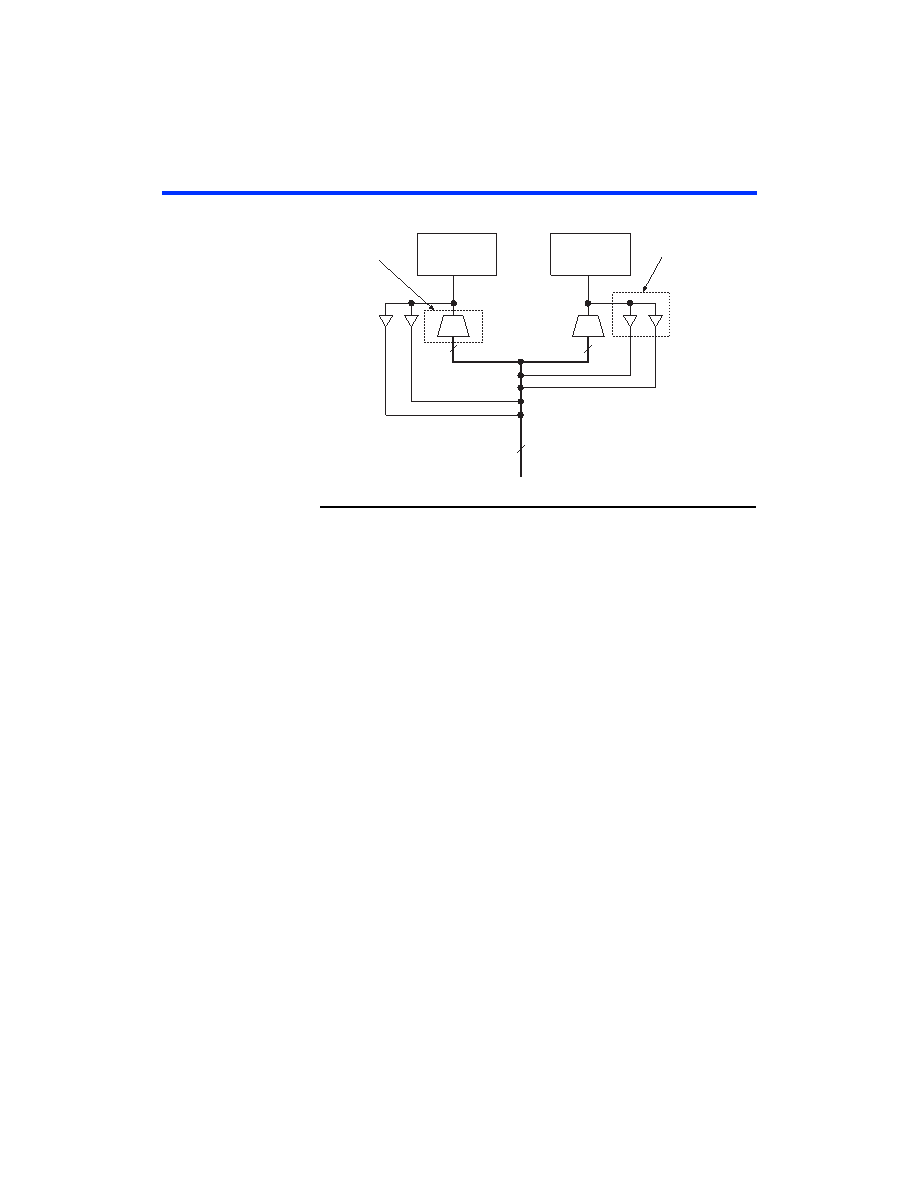
Figure 12. FLEX 8000 Column-to-IOE Connections
In addition to general-purpose I/O pins, FLEX 8000 devices have four
dedicated input pins. These dedicated inputs provide low-skew, device-
wide signal distribution, and are typically used for global clock, clear, and
preset control signals. The signals from the dedicated inputs are available
as control signals for all LABs and I/O elements in the device. The
dedicated inputs can also be used as general-purpose data inputs because
they can feed the local interconnect of each LAB in the device.
Signals enter the FLEX 8000 device either from the I/O pins that provide
general-purpose input capability or from the four dedicated inputs. The
IOEs are located at the ends of the row and column interconnect channels.
I/O pins can be used as input, output, or bidirectional pins. Each I/O pin
has a register that can be used either as an input register for external data
that requires fast setup times, or as an output register for data that
requires fast clock-to-output performance. The MAX+PLUS II Compiler
uses the programmable inversion option to invert signals automatically
from the row and column interconnect when appropriate.
The clock, clear, and output enable controls for the IOEs are provided by
a network of I/O control signals. These signals can be supplied by either
the dedicated input pins or by internal logic. The IOE control-signal paths
are designed to minimize the skew across the device. All control-signal
sources are buffered onto high-speed drivers that drive the signals around
the periphery of the device. This “peripheral bus” can be configured to
provide up to four output enable signals (10 in EPF81500A devices), and
up to two clock or clear signals. Figure 13 on page 22 shows how two
output enable signals are shared with one clock and one clear signal.
IOE
8
16
Column Interconnect
Each IOE is
driven by an
8-to-1
multiplexer.
Each IOE can drive
up to two column
signals.
相關(guān)PDF資料 |
PDF描述 |
|---|---|
| AGL400V2-CS196 | IC FPGA 1KB FLASH 400K 196-CSP |
| HMC36DRYN-S734 | CONN EDGECARD 72POS DIP .100 SLD |
| AGLP060V5-CSG289I | IC FPGA IGLOO PLUS 60K 289-CSP |
| AGLP060V5-CS289I | IC FPGA IGLOO PLUS 60K 289-CSP |
| HMC36DRYH-S734 | CONN EDGECARD 72POS DIP .100 SLD |
相關(guān)代理商/技術(shù)參數(shù) |
參數(shù)描述 |
|---|---|
| EPF8282ATC100-2N | 功能描述:FPGA - 現(xiàn)場(chǎng)可編程門陣列 FPGA - Flex 8000 26 LABs 78 IOs RoHS:否 制造商:Altera Corporation 系列:Cyclone V E 柵極數(shù)量: 邏輯塊數(shù)量:943 內(nèi)嵌式塊RAM - EBR:1956 kbit 輸入/輸出端數(shù)量:128 最大工作頻率:800 MHz 工作電源電壓:1.1 V 最大工作溫度:+ 70 C 安裝風(fēng)格:SMD/SMT 封裝 / 箱體:FBGA-256 |
| EPF8282ATC100-3 | 功能描述:FPGA - 現(xiàn)場(chǎng)可編程門陣列 FPGA - Flex 8000 26 LABs 78 IOs RoHS:否 制造商:Altera Corporation 系列:Cyclone V E 柵極數(shù)量: 邏輯塊數(shù)量:943 內(nèi)嵌式塊RAM - EBR:1956 kbit 輸入/輸出端數(shù)量:128 最大工作頻率:800 MHz 工作電源電壓:1.1 V 最大工作溫度:+ 70 C 安裝風(fēng)格:SMD/SMT 封裝 / 箱體:FBGA-256 |
| EPF8282ATC100-3N | 功能描述:FPGA - 現(xiàn)場(chǎng)可編程門陣列 FPGA - Flex 8000 26 LABs 78 IOs RoHS:否 制造商:Altera Corporation 系列:Cyclone V E 柵極數(shù)量: 邏輯塊數(shù)量:943 內(nèi)嵌式塊RAM - EBR:1956 kbit 輸入/輸出端數(shù)量:128 最大工作頻率:800 MHz 工作電源電壓:1.1 V 最大工作溫度:+ 70 C 安裝風(fēng)格:SMD/SMT 封裝 / 箱體:FBGA-256 |
| EPF8282ATC1004 | 制造商:ALTERA 功能描述:* |
| EPF8282ATC100-4 | 功能描述:FPGA - 現(xiàn)場(chǎng)可編程門陣列 FPGA - Flex 8000 26 LABs 78 IOs RoHS:否 制造商:Altera Corporation 系列:Cyclone V E 柵極數(shù)量: 邏輯塊數(shù)量:943 內(nèi)嵌式塊RAM - EBR:1956 kbit 輸入/輸出端數(shù)量:128 最大工作頻率:800 MHz 工作電源電壓:1.1 V 最大工作溫度:+ 70 C 安裝風(fēng)格:SMD/SMT 封裝 / 箱體:FBGA-256 |
發(fā)布緊急采購,3分鐘左右您將得到回復(fù)。