- 您現(xiàn)在的位置:買賣IC網(wǎng) > PDF目錄19913 > EPC1441LC20N (Altera)IC CONFIG DEVICE 440KBIT 20-PLCC PDF資料下載
參數(shù)資料
| 型號: | EPC1441LC20N |
| 廠商: | Altera |
| 文件頁數(shù): | 14/26頁 |
| 文件大?。?/td> | 0K |
| 描述: | IC CONFIG DEVICE 440KBIT 20-PLCC |
| 產品培訓模塊: | Three Reasons to Use FPGA's in Industrial Designs |
| 標準包裝: | 588 |
| 系列: | EPC |
| 可編程類型: | OTP |
| 存儲容量: | 440kb |
| 電源電壓: | 3 V ~ 3.6 V,4.75 V ~ 5.25 V |
| 工作溫度: | 0°C ~ 70°C |
| 封裝/外殼: | 20-LCC(J 形引線) |
| 供應商設備封裝: | 20-PLCC(9x9) |
| 包裝: | 管件 |
| 產品目錄頁面: | 604 (CN2011-ZH PDF) |
| 配用: | PLMJ1213-ND - PROGRAMMER ADAPTER 20 PIN J-LEAD |
| 其它名稱: | 544-1371-5 EPC1441LC20N-ND |
Pin Information
Page 21
Configuration Devices for SRAM-Based LUT Devices
January 2012
Altera Corporation
Pin Information
Table 20 lists the pin functions of the EPC1, EPC2, and EPC1441 devices during device
configuration.
f For more information about pin information of EPC devices, refer to the Enhanced
f For more information about pin information of EPCS devices, refer to the Serial
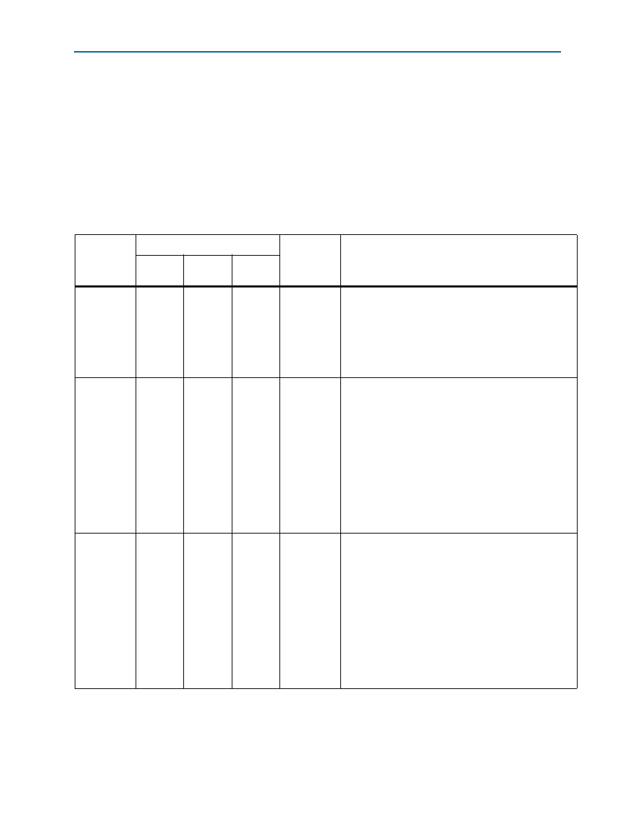
Table 20. EPC1, EPC2, and EPC1441 Device Pin Functions During Configuration (Part 1 of 3)
Pin Name
Pin Number
Pin Type
Description
8-Pin
PDIP (1)
20-Pin
PLCC
32-Pin
TQFP (2)
DATA
12
31
Output
Serial data output. The DATA pin connects to the DATA0 pin
of the FPGA. DATA is latched into the FPGA on the rising
edge of DCLK.
The DATA pin is tri-stated before configuration and when
the nCS pin is high. After configuration, the EPC2 device
drives DATA high, while the EPC1 and EPC1441 device
tri-state DATA.
DCLK
2
4
2
Bidirectional
Clock output when configuring with a single configuration
device or when the configuration device is the first
(master) device in a chain. Clock input for the next (slave)
configuration devices in a chain. The DCLK pin connects to
the DCLK pin of the FPGA.
Rising edges on DCLK increment the internal address
counter and present the next bit of data on the DATA pin.
The counter is incremented only if the OE input is held
high, the nCS input is held low, and all configuration data
has not been transferred to the target device.
After configuration or when OE is low, the EPC1, EPC2 and
EPC1441 device drive DCLK low.
OE
387
Open-drain
bidirectional
Output enable (active high) and reset (active low). The OE
pin connects to the nSTATUS pin of the FPGA.
A low logic level resets the address counter. A high logic
level enables DATA and the address counter to count. If this
pin is low (reset) during configuration, the internal
oscillator becomes inactive and DCLK drives low. For more
information, refer to “Error Detection Circuitry” on page 9.
The OE pin has an internal programmable 1-k
resistor in
EPC2 devices. If internal pull-up resistors are used, do not
use external pull-up resistors on these pins. You can
disable the internal pull-up resistors through the Disable
nCS
and OE pull-ups on configuration device option.
相關PDF資料 |
PDF描述 |
|---|---|
| EPC1213PC8 | IC CONFIG DEVICE 1MBIT 8-DIP |
| HBC49DRYI | CONN EDGECARD 98POS DIP .100 SLD |
| RSC05DRYI | CONN EDGECARD 10POS DIP .100 SLD |
| RBB106DHRT-S578 | CONN EDGECARD EXTEND 212POS .050 |
| HBC43DRAS | CONN EDGECARD 86POS R/A .100 SLD |
相關代理商/技術參數(shù) |
參數(shù)描述 |
|---|---|
| EPC1441LI20 | 功能描述:FPGA-配置存儲器 IC - Ser. Config Mem Flash 440Kb 8 MHz RoHS:否 制造商:Altera Corporation 存儲類型:Flash 存儲容量:1.6 Mbit 工作頻率:10 MHz 電源電壓-最大:5.25 V 電源電壓-最小:3 V 電源電流:50 uA 最大工作溫度:+ 85 C 最小工作溫度:- 40 C 安裝風格:SMD/SMT 封裝 / 箱體:PLCC-20 |
| EPC1441LI20N | 功能描述:FPGA-配置存儲器 IC - Ser. Config Mem Flash 440Kb 8 MHz RoHS:否 制造商:Altera Corporation 存儲類型:Flash 存儲容量:1.6 Mbit 工作頻率:10 MHz 電源電壓-最大:5.25 V 電源電壓-最小:3 V 電源電流:50 uA 最大工作溫度:+ 85 C 最小工作溫度:- 40 C 安裝風格:SMD/SMT 封裝 / 箱體:PLCC-20 |
| EPC1441PC8 | 功能描述:FPGA-配置存儲器 IC - Ser. Config Mem Flash 440Kb 8 MHz RoHS:否 制造商:Altera Corporation 存儲類型:Flash 存儲容量:1.6 Mbit 工作頻率:10 MHz 電源電壓-最大:5.25 V 電源電壓-最小:3 V 電源電流:50 uA 最大工作溫度:+ 85 C 最小工作溫度:- 40 C 安裝風格:SMD/SMT 封裝 / 箱體:PLCC-20 |
| EPC1441PC8N | 制造商:Altera Corporation 功能描述:CONFIGURATION DEVICE 400KBIT 8DIP |
| EPC1441PI8 | 功能描述:FPGA-配置存儲器 IC - Ser. Config Mem Flash 440Kb 8 MHz RoHS:否 制造商:Altera Corporation 存儲類型:Flash 存儲容量:1.6 Mbit 工作頻率:10 MHz 電源電壓-最大:5.25 V 電源電壓-最小:3 V 電源電流:50 uA 最大工作溫度:+ 85 C 最小工作溫度:- 40 C 安裝風格:SMD/SMT 封裝 / 箱體:PLCC-20 |
發(fā)布緊急采購,3分鐘左右您將得到回復。