- 您現(xiàn)在的位置:買賣IC網(wǎng) > PDF目錄357791 > EP9733-6 ACTIVE DELAY LINE, TRUE OUTPUT, SIP8 PDF資料下載
參數(shù)資料
| 型號: | EP9733-6 |
| 元件分類: | 延遲線 |
| 英文描述: | ACTIVE DELAY LINE, TRUE OUTPUT, SIP8 |
| 封裝: | SIP-8 |
| 文件頁數(shù): | 1/1頁 |
| 文件大小: | 14K |
| 代理商: | EP9733-6 |
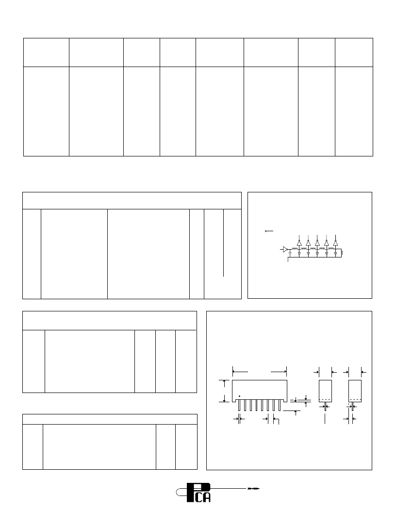
8 Pin SIL 5 Tap TTL Compatible Active Delay Lines
1.0 ± 0.5
1.5 ± 0.5
2.0 ± 1
2.5 ± 1
3.0 ± 1
4.0 ± 1.5
5.0
6.0
7.0
8.0
9.0
10.0
12.0
*4 ± 0.5
*6 ± 0.5
*8 ± 1.0
*10
*12
*16
*20
30
35
40
45
50
60
TAP DELAYS
±5% or ±2 nS
TOTAL DELAYS
±5% or ±2 nS
Part
Number
Pkg. A
Part
Number
Pkg. B
EP9677-4
EP9677-6
EP9677-8
EP9677-10
EP9677-12
EP9677-16
EP9677-20
EP9677-30
EP9677-35
EP9677-40
EP9677-45
EP9677-50
EP9677-60
EP9733-4
EP9733-6
EP9733-8
EP9733-10
EP9733-12
EP9733-16
EP9733-20
EP9733-30
EP9733-35
EP9733-40
EP9733-45
EP9733-50
EP9733-60
Whichever is greater. Delay times referenced from input to leading edges at 25°C, 5.0V, with no load.
*Delay times referenced from 1st tap
1st tap is the inherent delay: approx. 7 nS
TAP DELAYS
±5% or ±2 nS
TOTAL DELAYS
±5% or ±2 nS
Part
Number
Pkg. A
Part
Number
Pkg. B
15
20
25
30
35
40
50
60
70
80
90
100
75
100
125
150
175
200
250
300
350
400
450
500
EP9677-75
EP9677-100
EP9677-125
EP9677-150
EP9677-175
EP9677-200
EP9677-250
EP9677-300
EP9677-350
EP9677-400
EP9677-450
EP9677-500
EP9733-75
EP9733-100
EP9733-125
EP9733-150
EP9733-175
EP9733-200
EP9733-250
EP9733-300
EP9733-350
EP9733-400
EP9733-450
EP9733-500
VCC
VIH
VIL
IIK
IOH
IOL
PW*
d*
TA
Supply Voltage
High-Level Input Voltage
Low-Level Input Voltage
Input Clamp Current
High-Level Output Current
Low-Level Output Current
Pulse Width of Total Delay
Duty Cycle
Operating Free-Air Temperature
4.75
2.0
5.25
V
V
V
mA
mA
mA
%
%
°C
0.8
-18
-1.0
20
40
40
+70
0
*These two values are inter-dependent.
Recommended
Operating Conditions
Min
Max
Unit
EIN
PW
TRI
PRR
Pulse Input Voltage
Pulse Width % of Total Delay
Pulse Rise Time (0.75 - 2.4 Volts)
Pulse Repetition Rate @ Td
≤
200 nS
Pulse Repetition Rate @ Td > 200 nS
Supply Voltage
3.2
110
2.0
1.0
100
5.0
Volts
%
nS
MHz
KHz
Volts
VCC
Input Pulse Test Conditions @ 25° C
Unit
VOH
VOL
VIK
IIH
High-Level Output Voltage
Low-Level Output Voltage
Input Clamp Voltage
High-Level Input Current
VCC= min. VIL= max. IOH= max
VCC= min. VIH= min. IOL= max
VCC = min. II= IIK
VCC = max. VIN= 2.7V
VCC = max. VIN = 5.25V
VCC = max. VIN = 0.5V
2.7
V
V
V
μA
mA
mA
mA
0.5
-1.2V
50
1.0
-2
-100
IIL
IOS
Low-Level Input Current
Short Circuit Output Current VCC = max. VOUT = 0.
-40
(One output at a time)
VCC = max. VIN = OPEN
VCC = max. VIN= 0
Td
≤
500 nS (0.75 to 2.4 Volts)
VCC = max. VOH = 2.7V
VCC = max. VOL= 0.5V
ICCHHigh-Level Supply Current
ICCL
Low-Level Supply Current
TRO
Output Rise Time
NH
Fanout High-Level Output
NL
Fanout Low-Level Output
115
115
4
20 TTL LOAD
10 TTL LOAD
mA
mA
nS
DC Electrical Characteristics
Parameter
Test Conditions
Min Max Unit
Package Dimensions
Schematic
DSD9677 Rev. A 2/5/96
QAF-CSO1 Rev. B 8/25/94
Unless Otherwise Noted Dimensions in Inches
Tolerances:
Fractional = ± 1/32
.XX = ± .030 .XXX = ± .010
16799 SCHOENBORN ST.
NORTH HILLS, CA 91343
TEL: (818) 892-0761
FAX: (818) 894-5791
E L E C T R O N I C S I N C .
31
.020
Typ.
.820 Max.
.100 Typ.
.150 Min.
.015
Min.
.300 Max.
.010
Typ.
.190
Max
PCA
EP9677-4
Date Code
.190
Max
.
.010
Typ.
.065
Typ.
C
Pkg. A
Pkg. B
3
4
5
6
7
2
8
OUTPUT
GROUND
INPUT
1
VCC
相關(guān)PDF資料 |
PDF描述 |
|---|---|
| EPA054-600 | ACTIVE DELAY LINE, TRUE OUTPUT, DIP8 |
| EPA209-60 | SQUARE, 63 MHz, WAVEFORM GENERATION, PDIP5 |
| EPA247-550-RC | ACTIVE DELAY LINE, TRUE OUTPUT, PDSO14 |
| EPA247-75-RC | ACTIVE DELAY LINE, TRUE OUTPUT, PDSO14 |
| EPA3894 | 1 ELEMENT, 10 uH, GENERAL PURPOSE INDUCTOR, SMD |
相關(guān)代理商/技術(shù)參數(shù) |
參數(shù)描述 |
|---|---|
| EP9733-60 | 制造商:PCA 制造商全稱:PCA ELECTRONICS INC. 功能描述:8 Pin SIL 5 Tap TTL Compatible Active Delay Lines |
| EP9733-75 | 制造商:PCA 制造商全稱:PCA ELECTRONICS INC. 功能描述:8 Pin SIL 5 Tap TTL Compatible Active Delay Lines |
| EP9733-8 | 制造商:PCA 制造商全稱:PCA ELECTRONICS INC. 功能描述:8 Pin SIL 5 Tap TTL Compatible Active Delay Lines |
| EP9734-10 | 制造商:未知廠家 制造商全稱:未知廠家 功能描述:Tapped Delay Line |
| EP9734-11 | 制造商:未知廠家 制造商全稱:未知廠家 功能描述:Tapped Delay Line |
發(fā)布緊急采購,3分鐘左右您將得到回復。