- 您現在的位置:買賣IC網 > PDF目錄19320 > EP2S60F1020C4N (Altera)IC STRATIX II FPGA 60K 1020-FBGA PDF資料下載
參數資料
| 型號: | EP2S60F1020C4N |
| 廠商: | Altera |
| 文件頁數: | 413/768頁 |
| 文件大?。?/td> | 0K |
| 描述: | IC STRATIX II FPGA 60K 1020-FBGA |
| 產品培訓模塊: | Three Reasons to Use FPGA's in Industrial Designs |
| 標準包裝: | 6 |
| 系列: | Stratix® II |
| LAB/CLB數: | 3022 |
| 邏輯元件/單元數: | 60440 |
| RAM 位總計: | 2544192 |
| 輸入/輸出數: | 718 |
| 電源電壓: | 1.15 V ~ 1.25 V |
| 安裝類型: | 表面貼裝 |
| 工作溫度: | 0°C ~ 85°C |
| 封裝/外殼: | 1020-BBGA |
| 供應商設備封裝: | 1020-FBGA(33x33) |
| 配用: | 544-1700-ND - DSP KIT W/STRATIX II EP2S60N 544-1697-ND - NIOS II KIT W/STRATIX II EP2S60N |
| 其它名稱: | 544-1901 EP2S60F1020C4N-ND |
4–32
Altera Corporation
Stratix II Device Handbook, Volume 2
January 2008
On-Chip Termination
the external 50- resistors connected to the RUP and RDN pins and
dynamically enables or disables the transistors until they match.
Calibration happens at the end of the device configuration. Once the
calibration circuit finds the correct impedance, it powers down and stops
changing the characteristics of the drivers.
There are two separate sets of calibration circuits in the Stratix II and
Stratix II GX devices:
■
One calibration circuit for top banks 3 and 4
■
One calibration circuit for bottom banks 7 and 8
Calibration circuits rely on the external pull-up reference resistor (RUP)
and pull-down reference resistor (RDN) to achieve accurate on-chip series
and parallel termination. There is one pair of RUP and RDN pins in bank 4
for the calibration circuit for top I/O banks 3 and 4. Similarly, there is one
pair of RUP and RDN pins in bank 7 for the calibration circuit for bottom
I/O banks 7 and 8. Two banks share the same calibration circuitry, so they
must have the same VCCIO voltage if both banks enable on-chip series or
parallel termination with calibration. If banks 3 and 4 have different VCCIO
voltages, only bank 4 can enable on-chip series or parallel termination
with calibration because the RUP and RDN pins are located in bank 4.
Bank 3 still can use on-chip series termination, but without calibration.
The same rule applies to banks 7 and 8.
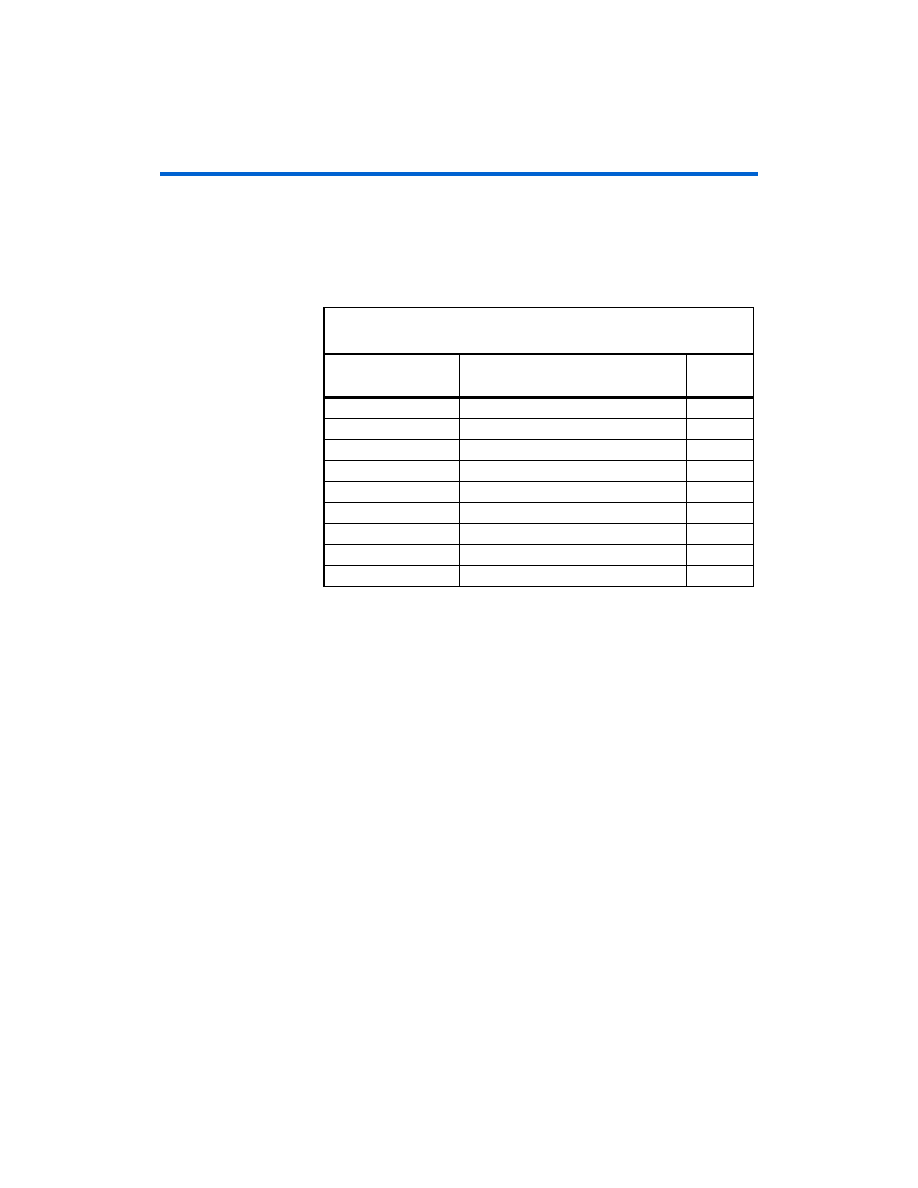
Table 4–7. Selectable I/O Drivers with On-Chip Parallel Termination with
Calibration
I/O Standard
On-Chip Parallel Termination Setting
(Column I/O)
Unit
SSTL-2 Class I
50
SSTL-2 Class II
50
SSTL-18 Class I
50
SSTL-18 Class II
50
1.8-V HSTL Class I
50
1.8-V HSTL Class II
50
1.5-V HSTL Class I
50
1.5-V HSTL Class II
50
1.2-V HSTL (1)
50
Note to Table 4–7:
(1)
1.2-V HSTL is only supported in I/O banks 4,7, and 8.
相關PDF資料 |
PDF描述 |
|---|---|
| VI-B62-EU-S | CONVERTER MOD DC/DC 15V 200W |
| IRS2552DSTRPBF | IC BALLAST CTLR CCFL/EEFL 16SOIC |
| LQG15HS6N8J02D | INDUCTOR 6.8NH 300MA 0402 |
| VJ1206A120KBCAT4X | CAP CER 12PF 200V 10% NP0 1206 |
| VJ1206A120KBEAT4X | CAP CER 12PF 500V 10% NP0 1206 |
相關代理商/技術參數 |
參數描述 |
|---|---|
| EP2S60F1020C5 | 功能描述:FPGA - 現場可編程門陣列 FPGA - Stratix II 3022 LABs 718 IOs RoHS:否 制造商:Altera Corporation 系列:Cyclone V E 柵極數量: 邏輯塊數量:943 內嵌式塊RAM - EBR:1956 kbit 輸入/輸出端數量:128 最大工作頻率:800 MHz 工作電源電壓:1.1 V 最大工作溫度:+ 70 C 安裝風格:SMD/SMT 封裝 / 箱體:FBGA-256 |
| EP2S60F1020C5N | 功能描述:FPGA - 現場可編程門陣列 FPGA - Stratix II 3022 LABs 718 IOs RoHS:否 制造商:Altera Corporation 系列:Cyclone V E 柵極數量: 邏輯塊數量:943 內嵌式塊RAM - EBR:1956 kbit 輸入/輸出端數量:128 最大工作頻率:800 MHz 工作電源電壓:1.1 V 最大工作溫度:+ 70 C 安裝風格:SMD/SMT 封裝 / 箱體:FBGA-256 |
| EP2S60F1020I4 | 功能描述:FPGA - 現場可編程門陣列 FPGA - Stratix II 3022 LABs 718 IOs RoHS:否 制造商:Altera Corporation 系列:Cyclone V E 柵極數量: 邏輯塊數量:943 內嵌式塊RAM - EBR:1956 kbit 輸入/輸出端數量:128 最大工作頻率:800 MHz 工作電源電壓:1.1 V 最大工作溫度:+ 70 C 安裝風格:SMD/SMT 封裝 / 箱體:FBGA-256 |
| EP2S60F1020I4N | 功能描述:FPGA - 現場可編程門陣列 FPGA - Stratix II 3022 LABs 718 IOs RoHS:否 制造商:Altera Corporation 系列:Cyclone V E 柵極數量: 邏輯塊數量:943 內嵌式塊RAM - EBR:1956 kbit 輸入/輸出端數量:128 最大工作頻率:800 MHz 工作電源電壓:1.1 V 最大工作溫度:+ 70 C 安裝風格:SMD/SMT 封裝 / 箱體:FBGA-256 |
| EP2S60F484C3 | 功能描述:FPGA - 現場可編程門陣列 FPGA - Stratix II 3022 LABs 334 IOs RoHS:否 制造商:Altera Corporation 系列:Cyclone V E 柵極數量: 邏輯塊數量:943 內嵌式塊RAM - EBR:1956 kbit 輸入/輸出端數量:128 最大工作頻率:800 MHz 工作電源電壓:1.1 V 最大工作溫度:+ 70 C 安裝風格:SMD/SMT 封裝 / 箱體:FBGA-256 |
發(fā)布緊急采購,3分鐘左右您將得到回復。