參數資料
| 型號: | EP2AGX65DF29I5N |
| 廠商: | Altera |
| 文件頁數: | 20/90頁 |
| 文件大?。?/td> | 0K |
| 描述: | IC ARRIA II GX FPGA 65K 780FBGA |
| 產品培訓模塊: | Three Reasons to Use FPGA's in Industrial Designs |
| 標準包裝: | 4 |
| 系列: | Arria II GX |
| LAB/CLB數: | 2530 |
| 邏輯元件/單元數: | 60214 |
| RAM 位總計: | 5371904 |
| 輸入/輸出數: | 364 |
| 電源電壓: | 0.87 V ~ 0.93 V |
| 安裝類型: | 表面貼裝 |
| 工作溫度: | -40°C ~ 100°C |
| 封裝/外殼: | 780-BBGA |
| 供應商設備封裝: | 780-FBGA(29x29) |
第1頁第2頁第3頁第4頁第5頁第6頁第7頁第8頁第9頁第10頁第11頁第12頁第13頁第14頁第15頁第16頁第17頁第18頁第19頁當前第20頁第21頁第22頁第23頁第24頁第25頁第26頁第27頁第28頁第29頁第30頁第31頁第32頁第33頁第34頁第35頁第36頁第37頁第38頁第39頁第40頁第41頁第42頁第43頁第44頁第45頁第46頁第47頁第48頁第49頁第50頁第51頁第52頁第53頁第54頁第55頁第56頁第57頁第58頁第59頁第60頁第61頁第62頁第63頁第64頁第65頁第66頁第67頁第68頁第69頁第70頁第71頁第72頁第73頁第74頁第75頁第76頁第77頁第78頁第79頁第80頁第81頁第82頁第83頁第84頁第85頁第86頁第87頁第88頁第89頁第90頁
Chapter 1: Device Datasheet for Arria II Devices
1–19
Electrical Characteristics
December 2013
Altera Corporation
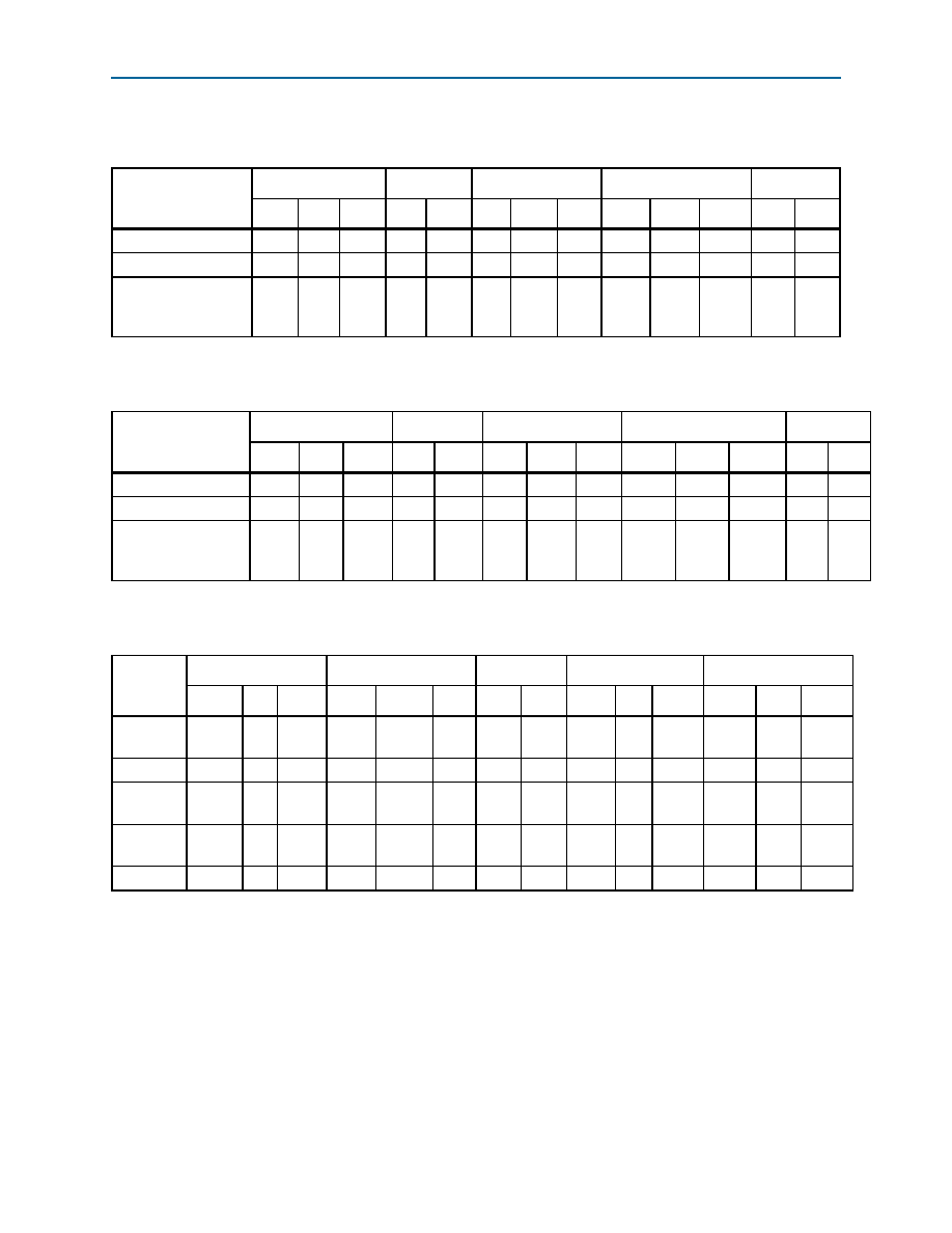
Table 1–30 lists the HSTL I/O standards for Arria II GX devices.
Table 1–31 lists the HSTL I/O standards for Arria II GZ devices.
Table 1–32 lists the differential I/O standard specifications for Arria II GX devices.
Table 1–30. Differential HSTL I/O Standards for Arria II GX Devices
I/O Standard
VCCIO (V)
VDIF(DC) (V)
VX(AC) (V)
VCM(DC) (V)
VDIF(AC) (V)
Min
Typ
Max
Min
Max
Min
Typ
Max
Min
Typ
Max
Min
Max
HSTL-18 Class I
1.71
1.8
1.89
0.2
—
0.85
—
0.95
0.88
—
0.95
0.4
—
HSTL-15 Class I, II
1.425
1.5
1.575
0.2
—
0.71
—
0.79
0.71
—
0.79
0.4
—
HSTL-12 Class I, II
1.14
1.2
1.26
0.16
—
0.5 ×
VCCIO
—
0.48
×
VCCIO
0.5 ×
VCCIO
0.52 ×
VCCIO
0.3
—
Table 1–31. Differential HSTL I/O Standards for Arria II GZ Devices
I/O Standard
VCCIO (V)
VDIF(DC) (V)
VX(AC) (V)
VCM(DC) (V)
VDIF(AC) (V)
Min
Typ
Max
Min
Max
Min
Typ
Max
Min
Typ
Max
Min
Max
HSTL-18 Class I
1.71
1.8
1.89
0.2
—
0.78
—
1.12
0.78
—
1.12
0.4
—
HSTL-15 Class I, II
1.425
1.5
1.575
0.2
—
0.68
—
0.9
0.68
—
0.9
0.4
—
HSTL-12 Class I, II
1.14
1.2
1.26
0.16
VCCIO
+ 0.3
—
0.5 ×
VCCIO
—
0.4 ×
VCCIO
0.5 ×
VCCIO
0.6 ×
VCCIO
0.3
VCCIO
+
0.48
Table 1–32. Differential I/O Standard Specifications for Arria II GX Devices (Note 1)
I/O
Standard
VCCIO (V)
VID (mV)
VOCM (V)
Min
Typ
Max
Min
Cond.
Max
Min
Max
Min
Typ
Max
Min
Typ
Max
2.5 V
LVDS
2.375
2.5
2.625
100
VCM =
1.25 V
—
0.05
1.80
0.247
—
0.6
1.125
1.25
1.375
RSDS (4)
2.375
2.5
2.625
—
0.1
0.2
0.6
0.5
1.2
1.4
Mini-LVDS
2.375
2.5
2.625
—
0.25
—
0.6
1
1.2
1.4
LVPECL
2.375
2.5
2.625
300
—
0.6
1.8
—
BLVDS (6)
2.375
2.5
2.625
100
—
Notes to Table 1–32:
(1) The 1.5 V PCML transceiver I/O standard specifications are described in “Transceiver Performance Specifications” on page 1–21.
(2) VIN range: 0 <= VIN <= 1.85 V.
(3) RL range: 90 <= RL <= 110 .
(4) The RSDS and mini-LVDS I/O standards are only supported for differential outputs.
(5) The LVPECL input standard is supported at the dedicated clock input pins (GCLK) only.
(6) There are no fixed VICM, VOD, and VOCM specifications for BLVDS. These specifications depend on the system topology.
相關PDF資料 |
PDF描述 |
|---|---|
| ABB91DHFN-S621 | EDGECARD 182PS .050 SMD W/O POST |
| 180-062-273L030 | CONN DB62 FEMALE HD CRIMP NICKEL |
| 180-044-273L020 | CONN DB44 FEMALE HD CRIMP NICKEL |
| ACB91DHFD-S621 | EDGECARD 182POS SMD W/O POST |
| 180-044-173L020 | CONN DB44 MALE HD CRIMP NICKEL |
相關代理商/技術參數 |
參數描述 |
|---|---|
| EP2AGX95DF25C4 | 功能描述:FPGA - 現場可編程門陣列 FPGA - Arria II GX 3747 LABs 260 IOs RoHS:否 制造商:Altera Corporation 系列:Cyclone V E 柵極數量: 邏輯塊數量:943 內嵌式塊RAM - EBR:1956 kbit 輸入/輸出端數量:128 最大工作頻率:800 MHz 工作電源電壓:1.1 V 最大工作溫度:+ 70 C 安裝風格:SMD/SMT 封裝 / 箱體:FBGA-256 |
| EP2AGX95DF25C4N | 功能描述:FPGA - 現場可編程門陣列 FPGA - Arria II GX 3747 LABs 260 IOs RoHS:否 制造商:Altera Corporation 系列:Cyclone V E 柵極數量: 邏輯塊數量:943 內嵌式塊RAM - EBR:1956 kbit 輸入/輸出端數量:128 最大工作頻率:800 MHz 工作電源電壓:1.1 V 最大工作溫度:+ 70 C 安裝風格:SMD/SMT 封裝 / 箱體:FBGA-256 |
| EP2AGX95DF25C5 | 功能描述:FPGA - 現場可編程門陣列 FPGA - Arria II GX 3747 LABs 260 IOs RoHS:否 制造商:Altera Corporation 系列:Cyclone V E 柵極數量: 邏輯塊數量:943 內嵌式塊RAM - EBR:1956 kbit 輸入/輸出端數量:128 最大工作頻率:800 MHz 工作電源電壓:1.1 V 最大工作溫度:+ 70 C 安裝風格:SMD/SMT 封裝 / 箱體:FBGA-256 |
| EP2AGX95DF25C5N | 功能描述:FPGA - 現場可編程門陣列 FPGA - Arria II GX 3747 LABs 260 IOs RoHS:否 制造商:Altera Corporation 系列:Cyclone V E 柵極數量: 邏輯塊數量:943 內嵌式塊RAM - EBR:1956 kbit 輸入/輸出端數量:128 最大工作頻率:800 MHz 工作電源電壓:1.1 V 最大工作溫度:+ 70 C 安裝風格:SMD/SMT 封裝 / 箱體:FBGA-256 |
| EP2AGX95DF25C6 | 功能描述:FPGA - 現場可編程門陣列 FPGA - Arria II GX 3747 LABs 260 IOs RoHS:否 制造商:Altera Corporation 系列:Cyclone V E 柵極數量: 邏輯塊數量:943 內嵌式塊RAM - EBR:1956 kbit 輸入/輸出端數量:128 最大工作頻率:800 MHz 工作電源電壓:1.1 V 最大工作溫度:+ 70 C 安裝風格:SMD/SMT 封裝 / 箱體:FBGA-256 |
發(fā)布緊急采購,3分鐘左右您將得到回復。