- 您現(xiàn)在的位置:買賣IC網(wǎng) > PDF目錄4457 > EP20K100EBC356-3 (Altera)IC APEX 20KE FPGA 100K 356-BGA PDF資料下載
參數(shù)資料
| 型號(hào): | EP20K100EBC356-3 |
| 廠商: | Altera |
| 文件頁數(shù): | 65/117頁 |
| 文件大小: | 0K |
| 描述: | IC APEX 20KE FPGA 100K 356-BGA |
| 產(chǎn)品培訓(xùn)模塊: | Three Reasons to Use FPGA's in Industrial Designs |
| 標(biāo)準(zhǔn)包裝: | 24 |
| 系列: | APEX-20K® |
| LAB/CLB數(shù): | 416 |
| 邏輯元件/單元數(shù): | 4160 |
| RAM 位總計(jì): | 53248 |
| 輸入/輸出數(shù): | 246 |
| 門數(shù): | 263000 |
| 電源電壓: | 1.71 V ~ 1.89 V |
| 安裝類型: | 表面貼裝 |
| 工作溫度: | 0°C ~ 85°C |
| 封裝/外殼: | 356-BGA |
| 供應(yīng)商設(shè)備封裝: | 356-BGA(35x35) |
| 其它名稱: | 544-1091 |
第1頁第2頁第3頁第4頁第5頁第6頁第7頁第8頁第9頁第10頁第11頁第12頁第13頁第14頁第15頁第16頁第17頁第18頁第19頁第20頁第21頁第22頁第23頁第24頁第25頁第26頁第27頁第28頁第29頁第30頁第31頁第32頁第33頁第34頁第35頁第36頁第37頁第38頁第39頁第40頁第41頁第42頁第43頁第44頁第45頁第46頁第47頁第48頁第49頁第50頁第51頁第52頁第53頁第54頁第55頁第56頁第57頁第58頁第59頁第60頁第61頁第62頁第63頁第64頁當(dāng)前第65頁第66頁第67頁第68頁第69頁第70頁第71頁第72頁第73頁第74頁第75頁第76頁第77頁第78頁第79頁第80頁第81頁第82頁第83頁第84頁第85頁第86頁第87頁第88頁第89頁第90頁第91頁第92頁第93頁第94頁第95頁第96頁第97頁第98頁第99頁第100頁第101頁第102頁第103頁第104頁第105頁第106頁第107頁第108頁第109頁第110頁第111頁第112頁第113頁第114頁第115頁第116頁第117頁
Altera Corporation
51
APEX 20K Programmable Logic Device Family Data Sheet
Notes to Table 15:
(1)
The PLL input frequency range for the EP20K100-1X device for 1x multiplication is 25 MHz to 175 MHz.
(2)
All input clock specifications must be met. The PLL may not lock onto an incoming clock if the clock specifications
are not met, creating an erroneous clock within the device.
(3)
During device configuration, the ClockLock and ClockBoost circuitry is configured first. If the incoming clock is
supplied during configuration, the ClockLock and ClockBoost circuitry locks during configuration, because the lock
time is less than the configuration time.
(4)
The jitter specification is measured under long-term observation.
(5)
If the input clock stability is 100 ps, tJITTER is 250 ps.
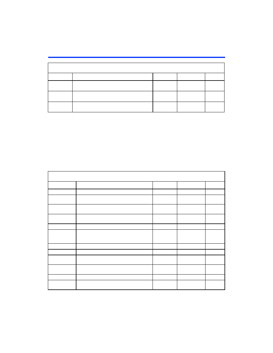
Table 16 summarizes the APEX 20K ClockLock and ClockBoost
parameters for -2 speed grade devices.
tSKEW
Skew delay between related
ClockLock/ClockBoost-generated clocks
500
ps
tJITTER
Jitter on ClockLock/ClockBoost-generated clock
200
ps
tINCLKSTB
Input clock stability (measured between adjacent
clocks)
50
ps
Table 15. APEX 20K ClockLock & ClockBoost Parameters for -1 Speed-Grade Devices (Part 2 of 2)
Symbol
Parameter
Min
Max
Unit
Table 16. APEX 20K ClockLock & ClockBoost Parameters for -2 Speed Grade Devices
Symbol
Parameter
Min
Max
Unit
fOUT
Output frequency
25
170
MHz
fCLK1
Input clock frequency (ClockBoost clock multiplication
factor equals 1)
25
170
MHz
fCLK2
Input clock frequency (ClockBoost clock multiplication
factor equals 2)
16
80
MHz
fCLK4
Input clock frequency (ClockBoost clock multiplication
factor equals 4)
10
34
MHz
tOUTDUTY
Duty cycle for ClockLock/ClockBoost-generated clock
40
60
%
fCLKDEV
Input deviation from user specification in the Quartus II
software (ClockBoost clock multiplication factor equals
one) (1)
25,000 (2)
PPM
tR
Input rise time
5ns
tF
Input fall time
5ns
tLOCK
Time required for ClockLock/ ClockBoost to acquire
lock (3)
10
s
tSKEW
Skew delay between related ClockLock/ ClockBoost-
generated clock
500
ps
tJITTER
Jitter on ClockLock/ ClockBoost-generated clock (4)
200
ps
tINCLKSTB
Input clock stability (measured between adjacent
clocks)
50
ps
相關(guān)PDF資料 |
PDF描述 |
|---|---|
| A3P1000-1FG256I | IC FPGA 1KB FLASH 1M 256-FBGA |
| AMM25DRYS | CONN EDGECARD 50POS DIP .156 SLD |
| 1-552076-1 | STR/REL COVRKIT 180DEG 24CON 2PC |
| AYM40DRSN | CONN EDGECARD 80POS DIP .156 SLD |
| AGM40DRSN | CONN EDGECARD 80POS DIP .156 SLD |
相關(guān)代理商/技術(shù)參數(shù) |
參數(shù)描述 |
|---|---|
| EP20K100EBC356-3ES | 制造商:未知廠家 制造商全稱:未知廠家 功能描述:FPGA |
| EP20K100EBC356-3N | 功能描述:FPGA - 現(xiàn)場可編程門陣列 CPLD - APEX 20K 416 Macro 246 IOs RoHS:否 制造商:Altera Corporation 系列:Cyclone V E 柵極數(shù)量: 邏輯塊數(shù)量:943 內(nèi)嵌式塊RAM - EBR:1956 kbit 輸入/輸出端數(shù)量:128 最大工作頻率:800 MHz 工作電源電壓:1.1 V 最大工作溫度:+ 70 C 安裝風(fēng)格:SMD/SMT 封裝 / 箱體:FBGA-256 |
| EP20K100EBI356-1ES | 制造商:未知廠家 制造商全稱:未知廠家 功能描述:FPGA |
| EP20K100EBI356-2ES | 制造商:未知廠家 制造商全稱:未知廠家 功能描述:FPGA |
| EP20K100EBI356-2X | 功能描述:IC APEX 20KE FPGA 100K 356-BGA RoHS:否 類別:集成電路 (IC) >> 嵌入式 - FPGA(現(xiàn)場可編程門陣列) 系列:APEX-20K® 產(chǎn)品變化通告:XC4000(E,L) Discontinuation 01/April/2002 標(biāo)準(zhǔn)包裝:24 系列:XC4000E/X LAB/CLB數(shù):100 邏輯元件/單元數(shù):238 RAM 位總計(jì):3200 輸入/輸出數(shù):80 門數(shù):3000 電源電壓:4.5 V ~ 5.5 V 安裝類型:表面貼裝 工作溫度:-40°C ~ 100°C 封裝/外殼:120-BCBGA 供應(yīng)商設(shè)備封裝:120-CPGA(34.55x34.55) |
發(fā)布緊急采購,3分鐘左右您將得到回復(fù)。