- 您現(xiàn)在的位置:買賣IC網(wǎng) > PDF目錄93338 > EDI7F233IMC 2x1Megx32 Flash Module(2x1Megx32閃速存儲器模塊) PDF資料下載
參數(shù)資料
| 型號: | EDI7F233IMC |
| 英文描述: | 2x1Megx32 Flash Module(2x1Megx32閃速存儲器模塊) |
| 中文描述: | 2x1Megx32閃存模塊(2x1Megx32閃速存儲器模塊) |
| 文件頁數(shù): | 1/3頁 |
| 文件大?。?/td> | 37K |
| 代理商: | EDI7F233IMC |
EDI7F33IMC
1Megx32
1
EDI7F33IMC Rev. 2 6/97 ECO #9019
Electronic Designs Incorporated
One Research Drive Westborough, MA 01581USA 508-366-5151 FAX 508-836-4850
Electronic Designs Europe Ltd. Shelley House, The Avenue Lightwater, Surrey GU18 5RF
United Kingdom 01276 472637 FAX: 01276 473748
http://www.electronic-designs.com
Features
1 Meg x 32 and 2 x 1 Meg x 32 Densities
Based on AMD - AM29F080 Flash Device
Fast Read Access Time - 90ns
5- Volt-Only Reprogramming
Sector Erase Architecture
Uniform sectors of 64 Kbytes each
Any combination of sectors can be erased
Also supports full chip erase
Sector Protection
Hardware method that disables any
combination of sectors from write or
erase operations
Embedded Erase Algorithms
Automatically preprograms and erases the
chip or any combination of sectors
Embedded Program Algorithms
Automatically programs and verifies data at
specified address
Data Polling and Toggle Bit feature for detection
of program or erase cycle completion
Low Power Dissipation
60mA per Device Active Current
10
A per Device CMOS Standby Current
Typical Endurance >100,000 Cycles
Single 5 Volt
±10% Supply
CMOS and TTL Compatible Inputs and Outputs
Commercial and Industrial Temperature Range
Package
80 Pin SIMM (JEDEC)
1Megx32 Flash Module
The EDI7F33IMC and EDI7F2331MC are orga-
nized as one and two banks of 1 meg x 32 respec-
tively. The modules are based on AMDs AM29F080
- 1Meg x 8 Flash device in TSOP packages which are
mounted on an FR4 substrate.
Both modules offer access times between 90 and
150ns allowing for operation of high-speed micropro-
cessors without wait states.
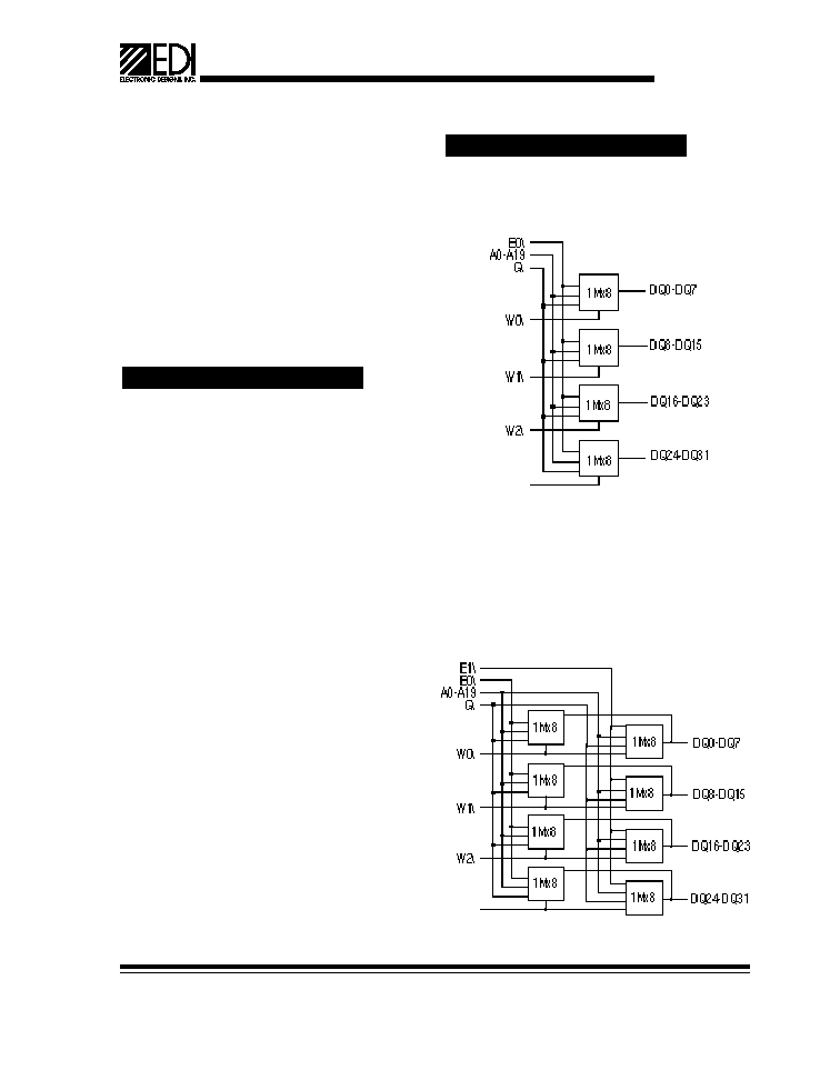
Block Diagrams
EDI7F33IMC-BNC
1Megx32 80 pin SIMM
EDI7F233IMC-BNC
2x1Megx32 80 pin SIMM
相關(guān)PDF資料 |
PDF描述 |
|---|---|
| EDI7F233IMV | 2x1Megx32 Flash Module(2x1Megx32閃速存儲器模塊) |
| EDI7F2341MC100BNC | EEPROM |
| EDI7F2341MC120BNC | EEPROM |
| EDI7F2341MC150BNC | EEPROM |
| EDI7F2341MC90BNC | EEPROM |
相關(guān)代理商/技術(shù)參數(shù) |
參數(shù)描述 |
|---|---|
| EDI7F233IMC100BNC | 制造商:未知廠家 制造商全稱:未知廠家 功能描述:1Megx32 Flash Module |
| EDI7F233IMC120BNC | 制造商:未知廠家 制造商全稱:未知廠家 功能描述:1Megx32 Flash Module |
| EDI7F233IMC150BNC | 制造商:未知廠家 制造商全稱:未知廠家 功能描述:1Megx32 Flash Module |
| EDI7F233LMC90BNC | 制造商:未知廠家 制造商全稱:未知廠家 功能描述:1Megx32 Flash Module |
| EDI7F2341MC100BNC | 制造商:WEDC 制造商全稱:White Electronic Designs Corporation 功能描述:1Mx32 FLASH MODULE |
發(fā)布緊急采購,3分鐘左右您將得到回復(fù)。