- 您現(xiàn)在的位置:買賣IC網(wǎng) > PDF目錄16261 > DS32512DK (Maxim Integrated Products)KIT DEMO FOR DS32512 PDF資料下載
參數(shù)資料
| 型號: | DS32512DK |
| 廠商: | Maxim Integrated Products |
| 文件頁數(shù): | 81/130頁 |
| 文件大?。?/td> | 0K |
| 描述: | KIT DEMO FOR DS32512 |
| 產(chǎn)品培訓(xùn)模塊: | Lead (SnPb) Finish for COTS Obsolescence Mitigation Program |
| 設(shè)計(jì)資源: | DS32512 Gerber Files |
| 標(biāo)準(zhǔn)包裝: | 1 |
| 主要目的: | 電信,線路接口單元(LIU) |
| 已用 IC / 零件: | DS32512 |
第1頁第2頁第3頁第4頁第5頁第6頁第7頁第8頁第9頁第10頁第11頁第12頁第13頁第14頁第15頁第16頁第17頁第18頁第19頁第20頁第21頁第22頁第23頁第24頁第25頁第26頁第27頁第28頁第29頁第30頁第31頁第32頁第33頁第34頁第35頁第36頁第37頁第38頁第39頁第40頁第41頁第42頁第43頁第44頁第45頁第46頁第47頁第48頁第49頁第50頁第51頁第52頁第53頁第54頁第55頁第56頁第57頁第58頁第59頁第60頁第61頁第62頁第63頁第64頁第65頁第66頁第67頁第68頁第69頁第70頁第71頁第72頁第73頁第74頁第75頁第76頁第77頁第78頁第79頁第80頁當(dāng)前第81頁第82頁第83頁第84頁第85頁第86頁第87頁第88頁第89頁第90頁第91頁第92頁第93頁第94頁第95頁第96頁第97頁第98頁第99頁第100頁第101頁第102頁第103頁第104頁第105頁第106頁第107頁第108頁第109頁第110頁第111頁第112頁第113頁第114頁第115頁第116頁第117頁第118頁第119頁第120頁第121頁第122頁第123頁第124頁第125頁第126頁第127頁第128頁第129頁第130頁
DS32506/DS32508/DS32512
54 of 130
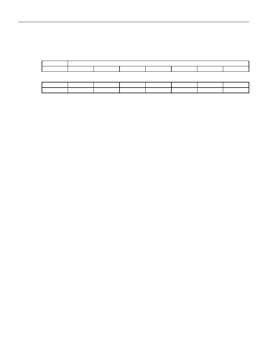
Register Name:
GLOBAL.CR2
Register Description:
Global Control Register #2
Register Address:
004h
Bit #
15
14
13
12
11
10
9
8
Name
—
CLAD[6:0]
Default
—
0
Bit #
7
6
5
4
3
2
1
0
Name
—
CLKD19
INTM
RAS
RAD
LSBCRE
GWRM
Default
0
Bits 14 to 8: CLAD I/O Mode (CLAD[6:0]).
Bit 5: CLKD Frequency is 19.44MHz (CLKD19).
This bit specifies the frequency to be output on CLKD when the
CLAD[3] configuration bit is high.
0 = 77.76MHz
1 = 19.44MHz
Bit 4: INT Pin Mode (INTM).
when an enabled interrupt source is active. See Section 8.10.
0 = Pin is high impedance when no enabled interrupts are active
1 = Pin drives high when no enabled interrupts are active
Bit 3: RDY/
ACK Select (RAS). This bit controls the microprocessor interface output pin RDY/ACK in Intel mode
(IFSEL = 100 or 110) and Motorola mode (IFSEL = 101 or 111).
0 = Normal operation: RDY in Intel mode and ACK in Motorola mode
1 = Reverse operation:
ACK in Intel mode and RDY in Motorola mode
Bit 2: RDY/
ACK Disable (RAD). This bit disables the microprocessor interface output pin RDY/ACK.
0 = Enable, normal operation
1 = Disable, tri-state
Bit 1: Latched Status Bit Clear-on-Read Enable (LSBCRE).
This bit determines when the latched status register
bits are cleared. See Section 8.8.5.
0 = Latched status register bits are cleared on a write
1 = Latched status register bits are cleared on a read
Bit 0: Global Write Mode (GWRM).
This bit enables the global write mode. When this bit is set, a write to a
register of any port causes a write to the same register in all the ports. In this mode register reads are not
supported and result in undefined data. See Section 8.8.6.
0 = Normal write mode
1 = Global write mode
相關(guān)PDF資料 |
PDF描述 |
|---|---|
| DS3253DK | KIT DEMO FOR DS3253 |
| DS26522DK | KIT DESIGN FOR DS26522 |
| EMM08DSEF-S13 | CONN EDGECARD 16POS .156 EXTEND |
| DS26528DK | KIT DESIGN FOR DS26528 |
| ESM12DRTN-S13 | CONN EDGECARD 24POS .156 EXTEND |
相關(guān)代理商/技術(shù)參數(shù) |
參數(shù)描述 |
|---|---|
| DS32512N | 功能描述:網(wǎng)絡(luò)控制器與處理器 IC 12-Port DS3/E3/STS-1 Line Interface Unit RoHS:否 制造商:Micrel 產(chǎn)品:Controller Area Network (CAN) 收發(fā)器數(shù)量: 數(shù)據(jù)速率: 電源電流(最大值):595 mA 最大工作溫度:+ 85 C 安裝風(fēng)格:SMD/SMT 封裝 / 箱體:PBGA-400 封裝:Tray |
| DS32512N# | 功能描述:網(wǎng)絡(luò)控制器與處理器 IC 12-Port DS3/E3/STS-1 Line Interface Unit RoHS:否 制造商:Micrel 產(chǎn)品:Controller Area Network (CAN) 收發(fā)器數(shù)量: 數(shù)據(jù)速率: 電源電流(最大值):595 mA 最大工作溫度:+ 85 C 安裝風(fēng)格:SMD/SMT 封裝 / 箱體:PBGA-400 封裝:Tray |
| DS32512N+ | 功能描述:網(wǎng)絡(luò)控制器與處理器 IC 12-Port DS3/E3/STS-1 Line Interface Unit RoHS:否 制造商:Micrel 產(chǎn)品:Controller Area Network (CAN) 收發(fā)器數(shù)量: 數(shù)據(jù)速率: 電源電流(最大值):595 mA 最大工作溫度:+ 85 C 安裝風(fēng)格:SMD/SMT 封裝 / 箱體:PBGA-400 封裝:Tray |
| DS32512NA2 | 制造商:Maxim Integrated Products 功能描述:DS32512 X12 DS3/E3 LIU REVA2 IND - Rail/Tube |
| DS32512NW | 功能描述:網(wǎng)絡(luò)控制器與處理器 IC RoHS:否 制造商:Micrel 產(chǎn)品:Controller Area Network (CAN) 收發(fā)器數(shù)量: 數(shù)據(jù)速率: 電源電流(最大值):595 mA 最大工作溫度:+ 85 C 安裝風(fēng)格:SMD/SMT 封裝 / 箱體:PBGA-400 封裝:Tray |
發(fā)布緊急采購,3分鐘左右您將得到回復(fù)。