- 您現(xiàn)在的位置:買賣IC網(wǎng) > PDF目錄97868 > DS2432P/T&R (MAXIM INTEGRATED PRODUCTS INC) 1K X 1 1-WIRE SERIAL EEPROM, PDSO6 PDF資料下載
參數(shù)資料
| 型號(hào): | DS2432P/T&R |
| 廠商: | MAXIM INTEGRATED PRODUCTS INC |
| 元件分類: | Programmable ROM |
| 英文描述: | 1K X 1 1-WIRE SERIAL EEPROM, PDSO6 |
| 封裝: | 0.150 INCH, TSOC-6 |
| 文件頁數(shù): | 11/16頁 |
| 文件大小: | 168K |
| 代理商: | DS2432P/T&R |
Abridged Data Sheet
DS2432
4 of 14
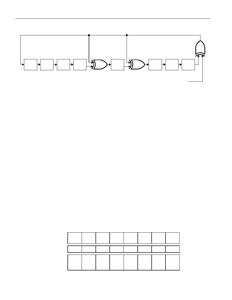
1-WIRE CRC GENERATOR Figure 4
X
0
X
1
X
2
X
3
X
4
X
5
X
6
X
7
X
8
Polynomial = X
8 + X5 + X4 + 1
1
st
STAGE
2
nd
STAGE
3
rd
STAGE
4
th
STAGE
6
th
STAGE
5
th
STAGE
7
th
STAGE
8
th
STAGE
INPUT DATA
MEMORY MAP
The DS2432 has four memory areas: data memory, secrets memory, register page with special function
registers and user-bytes, and a scratchpad. The data memory is organized in pages of 32 bytes. Secret,
register page and scratchpad are 8 bytes each. The scratchpad acts as a buffer when writing to the data
memory, loading the initial secret or when writing to the register page. For further details (including
Figure 5) refer to the full version of the data sheet.
ADDRESS REGISTERS AND TRANSFER STATUS
The DS2432 employs three address registers: TA1, TA2 and E/S (Figure 6). These registers are common
to many other 1-Wire devices but operate slightly differently with the DS2432. Registers TA1 and TA2
must be loaded with the target address to which the data will be written or from which data will be read.
Register E/S is a read-only transfer-status register, used to verify data integrity with write commands.
Since the scratchpad of the DS2432 is designed to accept data in blocks of eight bytes only, the lower
three bits of TA1 will be forced to 0 and the lower three bits of the E/S register (Ending Offset) will
always read 1. This indicates that all the data in the scratchpad will be used for a subsequent copying into
main memory or secret. Bit 5 of the E/S register, called PF or “partial byte flag”, is a logic-1 if the
number of data bits sent by the master is not an integer multiple of 8 or if the data in the scratchpad is not
valid due to a loss of power. A valid write to the scratchpad will clear the PF bit. Bits 3, 4 and 6 have no
function; they always read 1. The Partial Flag supports the master checking the data integrity after a
Write command. The highest valued bit of the E/S register, called AA or Authorization Accepted, acts as
a flag to indicate that the data stored in the scratchpad has already been copied to the target memory
address. Writing data to the scratchpad clears this flag.
ADDRESS REGISTERS Figure 6
Bit #
7
6
5
4
3
2
1
0
Target Address (TA1)
T7
T6
T5
T4
T3
T2
(0)
T1
(0)
T0
(0)
Target Address (TA2)
T15
T14
T13
T12
T11
T10
T9
T8
Ending Address with
Data Status (E/S)
(Read Only)
AA
1
PF
1
E2
(1)
E1
(1)
E0
(1)
相關(guān)PDF資料 |
PDF描述 |
|---|---|
| DS2432X | 1K X 1 1-WIRE SERIAL EEPROM, PBGA6 |
| DS2432P | 1K X 1 1-WIRE SERIAL EEPROM, PDSO6 |
| DS2433 | 512 X 8 1-WIRE SERIAL EEPROM, PBCY3 |
| DS2433X | 4K X 1 1-WIRE SERIAL EEPROM, UUC2 |
| DS2433S | 512 X 8 1-WIRE SERIAL EEPROM, PDSO8 |
相關(guān)代理商/技術(shù)參數(shù) |
參數(shù)描述 |
|---|---|
| DS2432P-W01+3T | 制造商:Maxim Integrated Products 功能描述:1KB PROTECTED 1-WIRE EEPROM WITH SHA-1 ENGINE - Tape and Reel |
| DS2432P-W0F+1T | 制造商:Maxim Integrated Products 功能描述: |
| DS2432Q-W01+4T | 制造商:Maxim Integrated Products 功能描述:1KB PROTECTED 1-WIRE EEPROM WITH SHA-1 E |
| DS2432X | 功能描述:電可擦除可編程只讀存儲(chǔ)器 RoHS:否 制造商:Atmel 存儲(chǔ)容量:2 Kbit 組織:256 B x 8 數(shù)據(jù)保留:100 yr 最大時(shí)鐘頻率:1000 KHz 最大工作電流:6 uA 工作電源電壓:1.7 V to 5.5 V 最大工作溫度:+ 85 C 安裝風(fēng)格:SMD/SMT 封裝 / 箱體:SOIC-8 |
| DS2432X+ | 功能描述:電可擦除可編程只讀存儲(chǔ)器 RoHS:否 制造商:Atmel 存儲(chǔ)容量:2 Kbit 組織:256 B x 8 數(shù)據(jù)保留:100 yr 最大時(shí)鐘頻率:1000 KHz 最大工作電流:6 uA 工作電源電壓:1.7 V to 5.5 V 最大工作溫度:+ 85 C 安裝風(fēng)格:SMD/SMT 封裝 / 箱體:SOIC-8 |
發(fā)布緊急采購,3分鐘左右您將得到回復(fù)。