- 您現(xiàn)在的位置:買賣IC網(wǎng) > PDF目錄97868 > DS2423P (MAXIM INTEGRATED PRODUCTS INC) SPECIALTY MEMORY CIRCUIT, PDSO6 PDF資料下載
參數(shù)資料
| 型號: | DS2423P |
| 廠商: | MAXIM INTEGRATED PRODUCTS INC |
| 元件分類: | Memory IC:Other |
| 英文描述: | SPECIALTY MEMORY CIRCUIT, PDSO6 |
| 封裝: | 3.70 X 4 MM, 1.50 MM HEIGHT, TSOC-6 |
| 文件頁數(shù): | 19/25頁 |
| 文件大小: | 581K |
| 代理商: | DS2423P |
DS2423
3 of 25
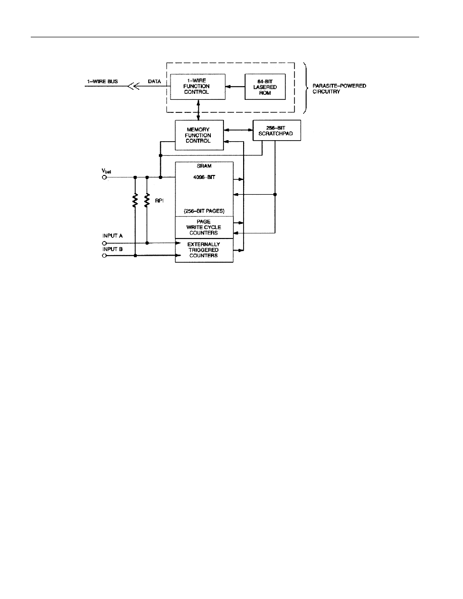
BLOCK DIAGRAM Figure 1
ADDRESS REGISTERS AND TRANSFER STATUS
Because of the serial data transfer, the DS2423 employs three address registers called TA1, TA2, and E/S
(Figure 6). Registers TA1 and TA2 must be loaded with the target address to which the data will be
written or from which data will be sent to the master upon a Read command. Register E/S acts like a byte
counter and Transfer Status register. It is used to verify data integrity with write commands. Therefore,
the master only has read access to this register. The lower 5 bits of the E/S register indicate the address of
the last byte that has been written to the scratchpad. This address is called Ending Offset. Bit 5 of the E/S
register, called PF or “partial byte flag,” is set if the number of data bits sent by the master is not an
integer multiple of 8. Bit 6 has no function; it always reads 0. Note that the lowest 5 bits of the target
address also determine the address within the scratchpad, where intermediate storage of data will begin.
This address is called byte offset. If the target address (TA1) for a Write command is 03CH for example,
then the scratchpad will store incoming data beginning at the byte offset 1CH and will be full after only 4
bytes. The corresponding ending offset in this example is 1FH. For best economy of speed and efficiency,
the target address for writing should point to the beginning of a new page, i.e., the byte offset will be 0.
Thus the full 32-byte capacity of the scratchpad is available, resulting also in the ending offset of 1FH.
However, it is possible to write one or several contiguous bytes somewhere within a page. The ending
offset together with the Partial Flag support the master checking the data integrity after a Write command.
The highest valued bit of the E/S register, called AA or Authorization Accepted, acts as a flag to indicate
that the data stored in the scratchpad has already been copied to the target memory address. Writing data
to the scratchpad clears this flag.
Not
Recommended
for
New
Design
相關(guān)PDF資料 |
PDF描述 |
|---|---|
| DS2423X | SPECIALTY MEMORY CIRCUIT, UUC |
| DS2423 | 4K X 1 STANDARD SRAM, PDSO6 |
| DS2422 | 1K X 1 STANDARD SRAM, PDSO6 |
| DS2430AP | 256 X 1 1-WIRE SERIAL EEPROM, PDSO6 |
| DS2430A | 32 X 8 1-WIRE SERIAL EEPROM, PBCY3 |
相關(guān)代理商/技術(shù)參數(shù) |
參數(shù)描述 |
|---|---|
| DS2423P/R | 制造商:DALLAS 制造商全稱:Dallas Semiconductor 功能描述:4kbit 1-Wire RAM with Counter |
| DS2423P/T | 制造商:DALLAS 制造商全稱:Dallas Semiconductor 功能描述:4kbit 1-Wire RAM with Counter |
| DS2423P/T&R | 功能描述:靜態(tài)隨機存取存儲器 RoHS:否 制造商:Cypress Semiconductor 存儲容量:16 Mbit 組織:1 M x 16 訪問時間:55 ns 電源電壓-最大:3.6 V 電源電壓-最小:2.2 V 最大工作電流:22 uA 最大工作溫度:+ 85 C 最小工作溫度:- 40 C 安裝風格:SMD/SMT 封裝 / 箱體:TSOP-48 封裝:Tray |
| DS2423P+ | 功能描述:靜態(tài)隨機存取存儲器 RoHS:否 制造商:Cypress Semiconductor 存儲容量:16 Mbit 組織:1 M x 16 訪問時間:55 ns 電源電壓-最大:3.6 V 電源電壓-最小:2.2 V 最大工作電流:22 uA 最大工作溫度:+ 85 C 最小工作溫度:- 40 C 安裝風格:SMD/SMT 封裝 / 箱體:TSOP-48 封裝:Tray |
| DS2423P+T&R | 制造商:Rochester Electronics LLC 功能描述: 制造商:DSC 功能描述: |
發(fā)布緊急采購,3分鐘左右您將得到回復(fù)。