- 您現(xiàn)在的位置:買(mǎi)賣(mài)IC網(wǎng) > PDF目錄295418 > DAC337-2 (SPECTRUM CONTROL INC) PARALLEL, 8 BITS INPUT LOADING, 20 us SETTLING TIME, 8-BIT DAC, CDIP14 PDF資料下載
參數(shù)資料
| 型號(hào): | DAC337-2 |
| 廠商: | SPECTRUM CONTROL INC |
| 元件分類: | DAC |
| 英文描述: | PARALLEL, 8 BITS INPUT LOADING, 20 us SETTLING TIME, 8-BIT DAC, CDIP14 |
| 封裝: | HERMETIC SEALED, DIP-14 |
| 文件頁(yè)數(shù): | 2/2頁(yè) |
| 文件大?。?/td> | 844K |
| 代理商: | DAC337-2 |
SPECIFICATIO N S
(Typical for all models @ +25 C and nominal power supplies unless otherwise noted)
SERIES
DA C337
TY PE
Fixed Ref., V olt, Output
DIGITA L INPUT
Resolution
8 Bits
Coding
DA C337-0
Complementary Binary
DA C337-1,6
Offset Binary
DA C337-2
Binary
Logic Compatibility
TTL, DTL, CM OS (from 5V supply)
V IH= 2.4V typ., 3.5V min.
V IH= 0.8V max.
A NA LOG OUTPUT
V oltage
DA C337-0
0 to –10V @ –5mA
DA C337-1
+5V +5mA
DA C337-2
0 to +10V @ +5mA
DA C337-6
±10V @ +5mA
Impedance
<0.1
REFERENCE
Internal
STA TIC PERFORM A NCE
Integral Linearity
±1/2 LSB, max.
Differential Linearity
±1/2 LSB, typ.; ±1 LSB.max.
DY NA M IC PERFORM A NCE
Settling Time to 1/2 LSB for Full Scale Change
DA C337–0,–1,–2
20s
DA C337-6
40s
For 1 LSB change
5s typ.; 10s max
Slew Rate
0.5V /s
STA BILITY (TMIN TO TMAX)
A ccuracy
1LSB
Linearity
±1/1 LSB, max.
Offset
±1 LSB, max.
POW ER SUPPLY
V oltage @ Current
+15V ±20% @ +6mA , max.
–15V ±20% @ –13mA , max.
Power Supply Rejection Ratio
+15V Supply, 0.1% FSR/V oIt
–15V Supply, 0.2% FSR/V oIt
TEM PERA TURE RA NGE
Operating
0C to +70C
Storage
–65C to +150C
M ECHA NICA L
Case Style
M etal or ceramic at
manufacturer's option
CA UTION: ESD (Electro-Static Discharge) sensitive device.
Permanent damage may occur when unconnected devices are
subjected to high energy electrostatic fields. Unused devices must
be stored in conductive foam or shunts. Protective foam should be
discharged to the destination socket before devices are removed.
Devices should be-handled at static safe workstations only. Unused
digital inputs must be grounded or tied to the logic supply voltage.
Unless otherwise noted, the supply voltage at any digital input
should never exceed the supply voltage by more than 0.5 volts or
go betow –0.5 volts. If this condition cannot be maintained, limit
input current on digital inputs by using series resistors or contact
SatCon for technical assistance.
Specifications subject to change without notice.
PIN
FUNCTION
PIN
FUNCTION
1
BIT1 (M SB)
14
BIT 8 (LSB)
2
BIT 2
13
BIT 7
3
BIT 3
12
BIT 6
4
BIT 4
11
BIT 5
5
OUTPUT
10
N.C.
6
GND
9
+15V
7
-15V
8
GND
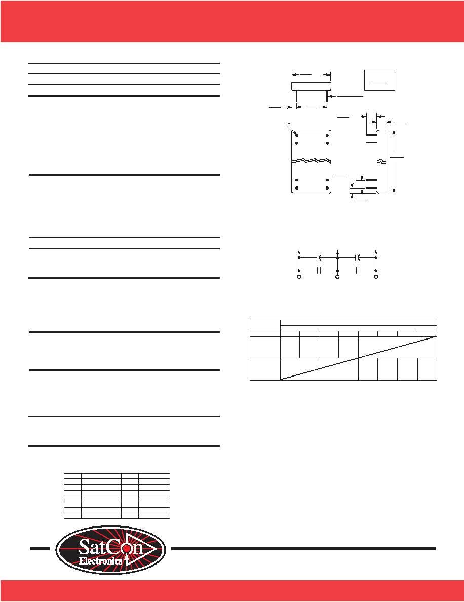
DA C337 -0, -1, -2, -6
0.475
(12.065)
M A X
0.10
(2.54)
0.300
(7.620)
0.010 ±0.002
(0.457 ±0.050)
0.220
(5.588)
M IN
0.100
(2.540)
TY P
RED DOT
INDICA TES PIN 1
0.155
(3.937)
M A X
0.800
(20.320)
M A X
0.10
(2.54)
TOP V IEW
DIM ENSIONS
INCHES
(mm)
APPLICATIO N IN FO RMATIO N
RECOM M ENDED POW ER SUPPLY BY -PA SS CIRCUIT
TRA NSFER CHA RA CTERISTICS
+15
– 15
1F
COM
0.01F
+
PIN 9
PIN 10
PIN 6,8
PIN 7,9
PIN 7 (8BIT)
PIN 8 (10 BIT)
TRA NSFER CHA RA CTERISTICS
A NA LOG OUTPUT
DA C337
INPUT PINS
11111111
1 0 0 0 0 0 0 0
11111111
1111111111
1 0 0 0 0 0 0 0 0 0
0 111111111
0 0 0 0 0 0 0 0 0 0
337 – 0
0V
– 4.961V
– 5V
– 9.961V
– 1
+5V
+0.040V
0
– 4.961V
– 2
– 9.961V
+5V
+4.961V
0V
– 6
+10V
+0.080V
0V
– 9.921V
0V
– 4.961V
5V
– 9.990V
+5V
+0.010V
0V
– 4.990V
+9.990V
+5V
+4.990V
0V
+10V
+0.020V
0V
– 9.980V
相關(guān)PDF資料 |
PDF描述 |
|---|---|
| DAC4815BP | QUAD, PARALLEL, 8 BITS INPUT LOADING, 3.5 us SETTLING TIME, 12-BIT DAC, PDIP28 |
| DAC56P | SERIAL INPUT LOADING, 1.5 us SETTLING TIME, 16-BIT DAC, PDIP16 |
| DAC602UB | PARALLEL, WORD INPUT LOADING, 0.015 us SETTLING TIME, 12-BIT DAC, PDSO28 |
| DAC716UB/1K | SERIAL INPUT LOADING, 6 us SETTLING TIME, 16-BIT DAC, PDSO16 |
| DAC716UL | SERIAL INPUT LOADING, 6 us SETTLING TIME, 16-BIT DAC, PDSO16 |
相關(guān)代理商/技術(shù)參數(shù) |
參數(shù)描述 |
|---|---|
| DAC337B-0 | 制造商:未知廠家 制造商全稱:未知廠家 功能描述:8-Bit Digital-to-Analog Converter |
| DAC337B-1 | 制造商:未知廠家 制造商全稱:未知廠家 功能描述:8-Bit Digital-to-Analog Converter |
| DAC337B-2 | 制造商:未知廠家 制造商全稱:未知廠家 功能描述:8-Bit Digital-to-Analog Converter |
| DAC337B-3 | 制造商:未知廠家 制造商全稱:未知廠家 功能描述:10-Bit Digital-to-Analog Converter |
| DAC337B-4 | 制造商:未知廠家 制造商全稱:未知廠家 功能描述:10-Bit Digital-to-Analog Converter |
發(fā)布緊急采購(gòu),3分鐘左右您將得到回復(fù)。