- 您現(xiàn)在的位置:買(mǎi)賣(mài)IC網(wǎng) > PDF目錄369679 > CYNSE70032 Network Processing PDF資料下載
參數(shù)資料
| 型號(hào): | CYNSE70032 |
| 英文描述: | Network Processing |
| 中文描述: | 網(wǎng)絡(luò)處理 |
| 文件頁(yè)數(shù): | 44/126頁(yè) |
| 文件大小: | 3302K |
| 代理商: | CYNSE70032 |
第1頁(yè)第2頁(yè)第3頁(yè)第4頁(yè)第5頁(yè)第6頁(yè)第7頁(yè)第8頁(yè)第9頁(yè)第10頁(yè)第11頁(yè)第12頁(yè)第13頁(yè)第14頁(yè)第15頁(yè)第16頁(yè)第17頁(yè)第18頁(yè)第19頁(yè)第20頁(yè)第21頁(yè)第22頁(yè)第23頁(yè)第24頁(yè)第25頁(yè)第26頁(yè)第27頁(yè)第28頁(yè)第29頁(yè)第30頁(yè)第31頁(yè)第32頁(yè)第33頁(yè)第34頁(yè)第35頁(yè)第36頁(yè)第37頁(yè)第38頁(yè)第39頁(yè)第40頁(yè)第41頁(yè)第42頁(yè)第43頁(yè)當(dāng)前第44頁(yè)第45頁(yè)第46頁(yè)第47頁(yè)第48頁(yè)第49頁(yè)第50頁(yè)第51頁(yè)第52頁(yè)第53頁(yè)第54頁(yè)第55頁(yè)第56頁(yè)第57頁(yè)第58頁(yè)第59頁(yè)第60頁(yè)第61頁(yè)第62頁(yè)第63頁(yè)第64頁(yè)第65頁(yè)第66頁(yè)第67頁(yè)第68頁(yè)第69頁(yè)第70頁(yè)第71頁(yè)第72頁(yè)第73頁(yè)第74頁(yè)第75頁(yè)第76頁(yè)第77頁(yè)第78頁(yè)第79頁(yè)第80頁(yè)第81頁(yè)第82頁(yè)第83頁(yè)第84頁(yè)第85頁(yè)第86頁(yè)第87頁(yè)第88頁(yè)第89頁(yè)第90頁(yè)第91頁(yè)第92頁(yè)第93頁(yè)第94頁(yè)第95頁(yè)第96頁(yè)第97頁(yè)第98頁(yè)第99頁(yè)第100頁(yè)第101頁(yè)第102頁(yè)第103頁(yè)第104頁(yè)第105頁(yè)第106頁(yè)第107頁(yè)第108頁(yè)第109頁(yè)第110頁(yè)第111頁(yè)第112頁(yè)第113頁(yè)第114頁(yè)第115頁(yè)第116頁(yè)第117頁(yè)第118頁(yè)第119頁(yè)第120頁(yè)第121頁(yè)第122頁(yè)第123頁(yè)第124頁(yè)第125頁(yè)第126頁(yè)
CYNSE70032
Document #: 38-02042 Rev. *E
Page 44 of 126
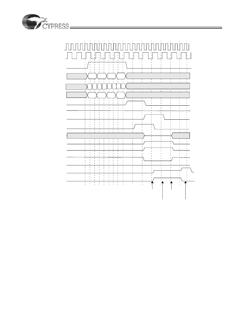
The following is the sequence of operation for a single 68-bit Search command (also refer to “Command and Command Param-
eters,” Subsection 12.2 on page 19).
Cycle A: The host ASIC drives CMDV high and applies Search command code (10) on CMD[1:0] signals. CMD[5:3] signals
must be driven with the index to the GMR pair for use in this Search operation. CMD[8:6] signals must be driven with the same
bits that will be driven on SADR[21:19] by this device if it has a hit. DQ[67:0] must be driven with the 68-bit data to be compared.
The CMD[2] signal must be driven to logic 0.
Cycle B: The host ASIC continues to drive CMDV high and applies Search command (10) on CMD[1:0]. CMD[5:2] must be
driven by the index of the comparand register pair for storing the 136-bit word presented on the DQ bus during cycles A and
B. CMD[8:6] signals must be driven with the index of the SSR that will be used for storing the address of the matching entry
and the hit flag (see page 14 for the description of SSR[0:7]). The DQ[67:0] continues to carry the 68-bit data to be compared.
Note
. For 68-bit searches, the host ASIC must supply the same 68-bit data on DQ[67:0] during both cycles A and B. The even
and odd GMR pairs selected for the compare must be programmed with the same value.
The logical 68-bit Search operation is shown in
Figure 13-22
. The entire table (31 devices of 68-bit entries) is compared to a 68-bit
word K (presented on the DQ bus in both cycles A and B of the command) using the GMR and the local mask bits. The effective
GMR is the 68-bit word specified by the identical value in both even and odd GMR pairs in each of the eight devices and selected
cycle
1
CLK2X
CMDV
CMD[1:0]
DQ
CE_L
ALE_L
OE_L
CMD[8:2]
Search2
Search4
WE_L
cycle
2
cycle
3
cycle
4
cycle
5
cycle
6
cycle
7
cycle
8
cycle
9
cycle
10
CFG = 00000000, HLAT = 001, TLSZ = 10, LRAM = 1, LDEV = 1.
Note: |(BHI[2:0)] stands for the boolean ‘OR’ of the entire bus BHI[2:0].
Note: |(LHI[6:0]) stands for the boolean ‘OR’ for the entire bus LHI[6:0].
Note: Each bit in BHO[2:0] is the same logical signal.
Note: Each bit in LHO[1:0] is the same logical signal.
PHS_L
SADR[21:0]
SSF
SSV
Search1
(Hit on some
device above.)
Search2
Search4
(Global miss;
this device
default driver.)
D1
D2
D3
D4
01
01
01
01
Search1
Search3
A B A B A B A B
z
z
z
0
0
LHO[1:0]
0
I(BHI[2:0])
0
Search3
(Hit on some
|(LHI[6:0])
0
BHO[2:0]
0
0
0
0
1
z
1
0
0
z
z
0
1
(Hit on some
device above.)
Figure 13-21. Timing Diagram for Device Number 6 in Block Number 3
(Device Number 30 in Depth-Cascaded Table)
相關(guān)PDF資料 |
PDF描述 |
|---|---|
| CYNSE70128 | Network Processing |
| CYNSE70256 | Network Processing |
| CZET101 | Clock Driver |
| CZEU101 | Quad Peripheral Driver |
| CZEZ101 | Triple Peripheral Driver |
相關(guān)代理商/技術(shù)參數(shù) |
參數(shù)描述 |
|---|---|
| CYNSE70032-66BGC | 制造商:CYPRESS 制造商全稱(chēng):Cypress Semiconductor 功能描述:Network Search Engine |
| CYNSE70032-66BGI | 制造商:CYPRESS 制造商全稱(chēng):Cypress Semiconductor 功能描述:Network Search Engine |
| CYNSE70032-83BGC | 制造商:CYPRESS 制造商全稱(chēng):Cypress Semiconductor 功能描述:Network Search Engine |
| CYNSE70064-50BGC | 制造商:Cypress Semiconductor 功能描述: |
| CYNSE70064-83BGC | 制造商:Cypress Semiconductor 功能描述: |
發(fā)布緊急采購(gòu),3分鐘左右您將得到回復(fù)。