- 您現(xiàn)在的位置:買賣IC網(wǎng) > PDF目錄357722 > CY62146VLL-70BAI x16 SRAM PDF資料下載
參數(shù)資料
| 型號(hào): | CY62146VLL-70BAI |
| 英文描述: | x16 SRAM |
| 中文描述: | x16的SRAM |
| 文件頁(yè)數(shù): | 5/10頁(yè) |
| 文件大小: | 153K |
| 代理商: | CY62146VLL-70BAI |
CY62147V18 MoBL2
5
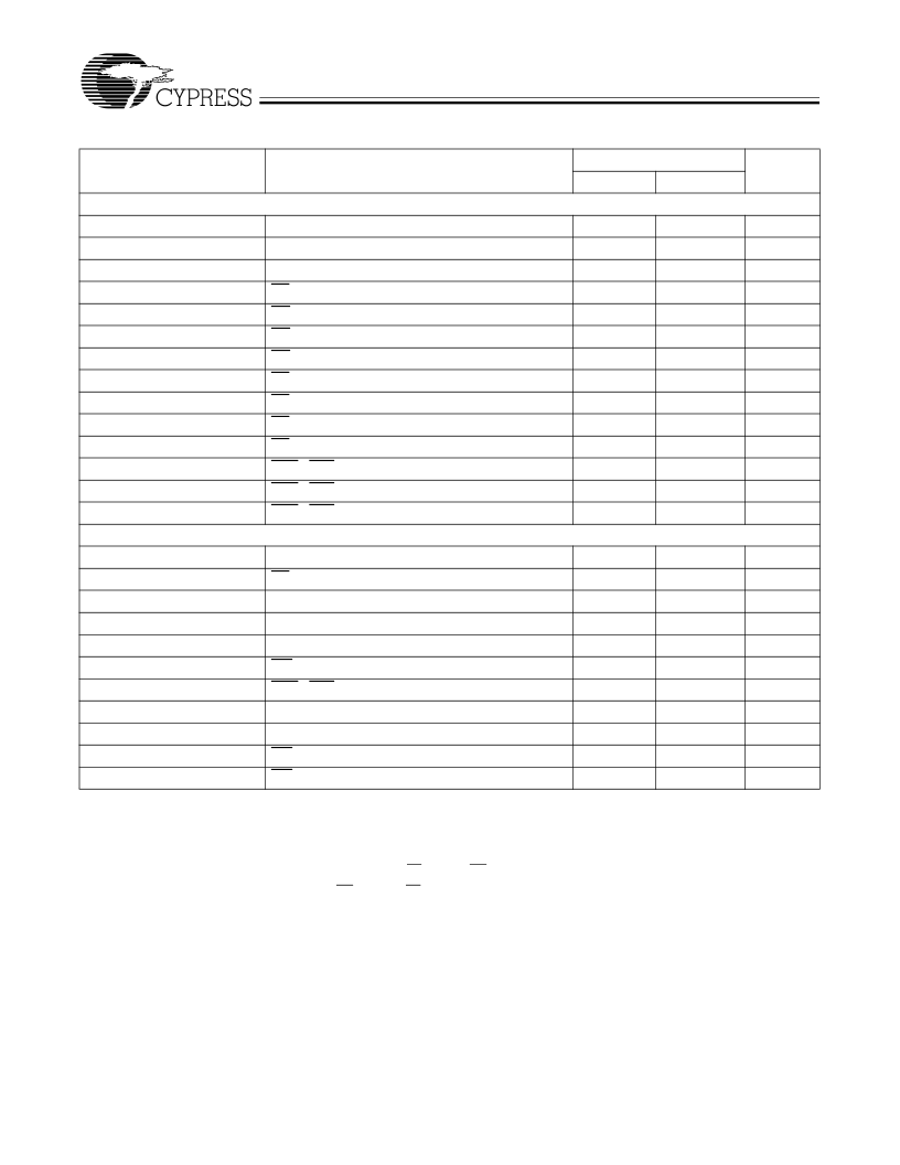
Switching Characteristics
Over the Operating Range
[5]
85 ns
Parameter
Description
Min.
Max.
Unit
READ CYCLE
t
RC
t
AA
t
OHA
t
ACE
t
DOE
t
LZOE
t
HZOE
t
LZCE
t
HZCE
t
PU
t
PD
t
DBE
t
LZBE[7]
t
HZBE
WRITE CYCLE
[9, 10]
t
WC
t
SCE
t
AW
t
HA
t
SA
t
PWE
t
BW
t
SD
t
HD
t
HZWE
t
LZWE
Notes:
5.
Test conditions assume signal transition time of 5 ns or less, timing reference levels of 1.5V, input pulse levels of 0 to V
CC(typ.)
, and output loading of the
specified I
/I
and 30 pF load capacitance.
6.
At any given temperature and voltage condition, t
is less than t
LZCE
, t
HZOE
is less than t
LZOE
, and t
HZWE
is less than t
LZWE
for any given device.
7.
If both byte enables are toggled together this value is 10ns
8.
t
, t
, and t
are specified with C
= 5 pF as in part (b) of AC Test Loads. Transition is measured
±
500 mV from steady-state voltage.
9.
The internal write time of the memory is defined by the overlap of CE LOW and WE LOW. Both signals must be LOW to initiate a write and either signal can
terminate a write by going HIGH. The data input set-up and hold timing should be referenced to the rising edge of the signal that terminates the write.
10. The minimum write cycle time for Write Cycle #3 (WE controlled, OE LOW) is the sum of t
HZWE
and t
SD
.
Read Cycle Time
85
ns
Address to Data Valid
85
ns
Data Hold from Address Change
10
ns
CE LOW to Data Valid
85
ns
OE LOW to Data Valid
OE LOW to Low Z
[6, 8]
OE HIGH to High Z
[8]
CE LOW to Low Z
[6]
CE HIGH to High Z
[6, 8]
45
ns
5
ns
25
ns
10
ns
25
ns
CE LOW to Power-Up
0
ns
CE HIGH to Power-Down
85
ns
BHE / BLE LOW to Data Valid
85
ns
BHE / BLE LOW to Low Z
5
ns
BHE / BLE HIGH to High Z
25
ns
Write Cycle Time
85
ns
CE LOW to Write End
75
ns
Address Set-Up to Write End
75
ns
Address Hold from Write End
0
ns
Address Set-Up to Write Start
0
ns
WE Pulse Width
65
ns
BHE / BLE Pulse Width
75
ns
Data Set-Up to Write End
45
ns
Data Hold from Write End
WE LOW to High Z
[6, 8]
WE HIGH to Low Z
[6]
0
ns
35
ns
10
ns
相關(guān)PDF資料 |
PDF描述 |
|---|---|
| CY62147BV18LL-70BAI | x16 SRAM |
| CY62148LL-100SI | x8 SRAM |
| CY62148LL-100ZSC | x8 SRAM |
| CY62148LL-100ZSI | x8 SRAM |
| CY62148LL-70SI | x8 SRAM |
相關(guān)代理商/技術(shù)參數(shù) |
參數(shù)描述 |
|---|---|
| CY62146VLL-70BAIT | 制造商:Cypress Semiconductor 功能描述:SRAM Chip Async Single 3V 4M-Bit 256K x 16 70ns 48-Pin FBGA T/R |
| CY62146VLL-70ZI | 制造商:Cypress Semiconductor 功能描述: |
| CY62146VLL-70ZS1 | 制造商:Cypress Semiconductor 功能描述: |
| CY621472E30LL-45ZSXI | 功能描述:靜態(tài)隨機(jī)存取存儲(chǔ)器 4-Mbit Static RAM RoHS:否 制造商:Cypress Semiconductor 存儲(chǔ)容量:16 Mbit 組織:1 M x 16 訪問(wèn)時(shí)間:55 ns 電源電壓-最大:3.6 V 電源電壓-最小:2.2 V 最大工作電流:22 uA 最大工作溫度:+ 85 C 最小工作溫度:- 40 C 安裝風(fēng)格:SMD/SMT 封裝 / 箱體:TSOP-48 封裝:Tray |
| CY621472E30LL-45ZSXIT | 功能描述:靜態(tài)隨機(jī)存取存儲(chǔ)器 4-Mbit Static RAM RoHS:否 制造商:Cypress Semiconductor 存儲(chǔ)容量:16 Mbit 組織:1 M x 16 訪問(wèn)時(shí)間:55 ns 電源電壓-最大:3.6 V 電源電壓-最小:2.2 V 最大工作電流:22 uA 最大工作溫度:+ 85 C 最小工作溫度:- 40 C 安裝風(fēng)格:SMD/SMT 封裝 / 箱體:TSOP-48 封裝:Tray |
發(fā)布緊急采購(gòu),3分鐘左右您將得到回復(fù)。